mitac 8599.pdf - tim.id.au
mitac 8599.pdf - tim.id.au
mitac 8599.pdf - tim.id.au

Create successful ePaper yourself
Turn your PDF publications into a flip-book with our unique Google optimized e-Paper software.
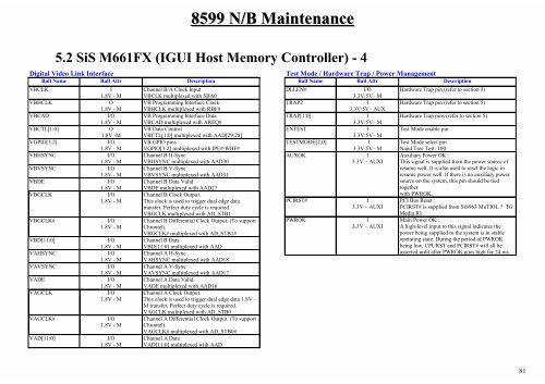
8599 N/B Maintenance<br />
5.2 SiS M661FX (IGUI Host Memory Controller) - 4<br />
Digital V<strong>id</strong>eo Link Interface<br />
Ball Name Ball Attr Description<br />
VBCLK I<br />
1.8V - M<br />
VBHCLK O<br />
1.8V - M<br />
VBCAD I/O<br />
1.8V - M<br />
VBCTL[1:0] O<br />
1.8V -M<br />
VGPIO[3:2] I/O<br />
1.8V - M<br />
VBHSYNC I/O<br />
1.8V - M<br />
VBVSYNC I/O<br />
1.8V - M<br />
VBDE I/O<br />
1.8V - M<br />
VBGCLK I/O<br />
1.8V - M<br />
VBGCLK# I/O<br />
1.8V - M<br />
VBD[11:0] I/O<br />
1.8V - M<br />
VAHSYNC I/O<br />
1.8V - M<br />
VAVSYNC I/O<br />
1.8V - M<br />
VADE I/O<br />
1.8V - M<br />
VAGCLK I/O<br />
1.8V - M<br />
VAGCLK# I/O<br />
1.8V - M<br />
VAD[11:0] I/O<br />
1.8V - M<br />
Channel B/A Clock Input<br />
VBCLK multiplexed with SBA0<br />
VB Programming Interface Clock<br />
VBHCLK multiplexed with RBF#<br />
VB Programming Interface Data<br />
VBCAD multiplexed with AREQ#<br />
VB Data Control<br />
VBCTL[1:0] multiplexed with AAD[29:28]<br />
VB GPIO pins<br />
VGPIO[3:2] multiplexed with IPE#/WBF#<br />
Channel B H-Sync<br />
VBHSYNC multiplexed with AAD30<br />
Channel B V-Sync<br />
VBVSYNC multiplexed with AAD31<br />
Channel B Data Val<strong>id</strong><br />
VBDE multiplexed with AAD27<br />
Channel B Clock Output.<br />
This clock is used to trigger dual edge data<br />
transfer. Perfect duty cycle is required.<br />
VBGCLK multiplexed with AD_STB1<br />
Channel B Differential Clock Output. (To support<br />
Chrontel).<br />
VBGCLK# multiplexed with AD_STB1#<br />
Channel B Data<br />
VBD[11:0] multiplexed with AAD<br />
Channel A H-Sync<br />
VAHSYNC multiplexed with AAD18<br />
Channel A V-Sync<br />
VAVSYNC multiplexed with AAD17<br />
Channel A Data Val<strong>id</strong><br />
VADE multiplexed with AAD16<br />
Channel A Clock Output.<br />
This clock is used to trigger dual edge data 1.8V –<br />
M transfer. Perfect duty cycle is required.<br />
VAGCLK multiplexed with AD_STB0<br />
Channel A Differential Clock Output. (To support<br />
Chrontel).<br />
VAGCLK# multiplexed with AD_STB0#<br />
Channel A Data<br />
VAD[11:0] multiplexed with AAD<br />
Test Mode / Hardware Trap / Power Management<br />
Ball Name Ball Attr Description<br />
DLLEN# I/O<br />
3.3V/5V– M<br />
TRAP2 I<br />
3.3V/5V– AUX<br />
TRAP[1:0] I<br />
3.3V/5V– M<br />
ENTEST I<br />
3.3V/5V– M<br />
TESTMODE[2:0] I<br />
3.3V/5V– M<br />
AUXOK I<br />
3.3V – AUXI<br />
PCIRST# I<br />
3.3V – AUXI<br />
PWROK I<br />
3.3V – AUXI<br />
Hardware Trap pin (refer to section 5)<br />
Hardware Trap pin (refer to section 5)<br />
Hardware Trap pins (refer to section 5)<br />
Test Mode enable pin<br />
Test Mode select pin<br />
Nand Tree Test: 100<br />
Auxiliary Power OK :<br />
This signal is supplied from the power source of<br />
resume well. It is also used to reset the logic in<br />
resume power well. If there is no <strong>au</strong>xiliary power<br />
source on the system, this pin should be tied<br />
together<br />
with PWROK.<br />
PCI Bus Reset :<br />
PCIRST# is supplied from SiS963 MuTIOL ? ?1G<br />
Media IO.<br />
Main Power OK :<br />
A high-level input to this signal indicates the<br />
power being supplied to the system is in stable<br />
operating state. During the period of PWROK<br />
being low, CPURST and PCIRST# will all be<br />
asserted until after PWROK goes high for 24 ms.<br />
81