mitac 8599.pdf - tim.id.au
mitac 8599.pdf - tim.id.au
mitac 8599.pdf - tim.id.au

Create successful ePaper yourself
Turn your PDF publications into a flip-book with our unique Google optimized e-Paper software.
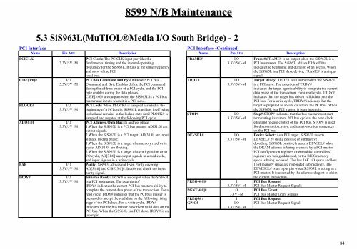
8599 N/B Maintenance<br />
5.3 SiS963L(MuTIOL®Media I/O South Br<strong>id</strong>ge) - 2<br />
PCI Interface<br />
Name Pin Attr Description<br />
PCICLK I<br />
3.3V/5V -M<br />
C/BE[3:0]# I/O<br />
3.3V/5V -M<br />
PLOCK# I/O<br />
3.3V/5V -M<br />
AD[31:0] I/O<br />
3.3V/5V -M<br />
PAR I/O<br />
3.3V/5V -M<br />
IRDY# I/O<br />
3.3V/5V -M<br />
PCI Clock: The PCICLK input prov<strong>id</strong>es the<br />
fundamental <strong>tim</strong>ing and the internal operating<br />
frequency for the SiS963L. It runs at the same frequency<br />
and skew of the PCI<br />
local bus.<br />
PCI Bus Command and Byte Enables: PCI Bus<br />
Command and Byte Enables define the PCI command<br />
during the address phase of a PCI cycle, and the PCI<br />
byte enables during the data phases.<br />
C/BE[3:0]# are outputs when the SiS963L is a PCI bus<br />
master and inputs when it is a PCI slave.<br />
PCI Lock: When PLOCK# is sampled asserted at the<br />
beginning of a PCI cycle, SiS963L cons<strong>id</strong>ers itself being<br />
locked and remains in the locked state until PLOCK# is<br />
sampled and negated at the following PCI cycle.<br />
PCI Address /Data Bus: In address phase:<br />
1.When the SiS963L is a PCI bus master, AD[31:0] are<br />
output signals.<br />
2.When the SiS963L is a PCI target, AD[31:0] are input<br />
signals. In data phase:<br />
1.When the SiS963L is a target of a memory read/write<br />
cycle, AD[31:0] are floating.<br />
2.When the SiS963L is a target of a configuration or an<br />
I/O cycle, AD[31:0] are output signals in a read cycle,<br />
and input signals in a write cycle.<br />
Parity: SiS963L drives out Even Parity covering<br />
AD[31:0] and C/BE[3:0]#. It does not check the input<br />
parity signal.<br />
Initiator Ready: IRDY# is an output when the SiS963L<br />
is a PCI bus master. The assertion of<br />
IRDY# indicates the current PCI bus master's ability to<br />
complete the current data phase of the transaction. For a<br />
read cycle, IRDY# indicates that the PCI bus master is<br />
prepared to accept the read data on the following rising<br />
edge of the PCI clock. For a write cycle, IRDY#<br />
indicates that the bus master has driven val<strong>id</strong> data on the<br />
PCI bus. When the SiS963L is a PCI slave, IRDY# is an<br />
input pin.<br />
PCI Interface (Continued)<br />
Name Pin Attr Description<br />
FRAME# I/O<br />
3.3V/5V -M<br />
TRDY# I/O<br />
3.3V/5V -M<br />
STOP# I/O<br />
3.3V/5V -M<br />
DEVSEL# I/O<br />
3.3V/5V -M<br />
PREQ[4:0]# I<br />
3.3V/5V -M<br />
PGNT[4:0]# O<br />
3.3V –M<br />
PREQ5# /<br />
I<br />
GPIO5<br />
I/O<br />
3.3V/5V- M<br />
Frame#:FRAME# is an output when the SiS963L is a<br />
PCI bus master. The SiS963L drives FRAME# to<br />
indicate the beginning and duration of an access. When<br />
the SiS963L is a PCI slave device, FRAME# is an input<br />
signal.<br />
Target Ready: TRDY# is an output when the SiS963L<br />
is a PCI slave. The assertion of TRDY#<br />
indicates the target agent's ability to complete the current<br />
data phase of the transaction. For a read cycle, TRDY#<br />
indicates that the target has driven val<strong>id</strong> data onto the<br />
PCI bus. For a write cycle, TRDY# indicates that the<br />
target is prepared to accept data from the PCI bus. When<br />
the SiS963L is a PCI master, it is an input pin.<br />
Stop#:STOP# indicates that the bus master must start<br />
terminating its current PCI bus cycle at the next clock<br />
edge and release control of the PCI bus. STOP# is used<br />
for disconnection, retry, and target-abortion sequences<br />
on the PCI bus.<br />
Device Select: As a PCI target, SiS963L asserts<br />
DEVSEL# by doing positive or subtractive<br />
decoding. SiS963L positively asserts DEVSEL# when<br />
the DRAM address is being accessed by a PCI master,<br />
PCI configuration registers or embedded controllers’<br />
registers are being addressed, or the BIOS memory<br />
space is being accessed. The low 16K I/O space and low<br />
16M memory space are responded subtractively. The<br />
DEVESEL# is an input pin when SiS963L is acting as a<br />
PCI master. It is asserted by the addressed agent to claim<br />
the current transaction.<br />
PCI Bus Request:<br />
PCI Bus Master Request Signals<br />
PCI Bus Grant:<br />
PCI Bus Master Grant Signals<br />
PCI Bus Request:<br />
PCI Bus Master Request Signal<br />
84