- Page 1 and 2:
Design Reference August 2002 Advanc
- Page 3 and 4:
Forward Everyone interested in anal
- Page 5 and 6:
Contents Contents 1 The Op Amp’s
- Page 7 and 8:
Contents 10 Op Amp Noise Theory and
- Page 9 and 10:
Contents 14.4.3 AC Application Erro
- Page 11 and 12:
Contents 17.7.1 Through-Hole Consid
- Page 13 and 14:
Figures Figures 2-1 Ohm’s Law App
- Page 15 and 16:
Figures 7-5 TL08X Frequency and Tim
- Page 17 and 18:
Figures 13-12 Differential Amplifie
- Page 19 and 20:
Figures 16-41 Comparison of Q Betwe
- Page 21 and 22:
Figures A-37 Basic Wien Bridge Osci
- Page 23 and 24:
Examples Examples 16-1 First-Order
- Page 25 and 26:
Chapter 1 The Op Amp’s Place In T
- Page 27 and 28:
The first signal conditioning op am
- Page 29 and 30:
Chapter 2 Review of Circuit Theory
- Page 31 and 32:
Voltage Divider Rule source, throug
- Page 33 and 34:
Thevenin’s Theorem 2.5 Thevenin
- Page 35 and 36:
Thevenin’s Theorem V OUT V TH R
- Page 37 and 38:
Calculation of a Saturated Transist
- Page 39 and 40:
Transistor Amplifier 2 V (from 8 V
- Page 41 and 42:
Chapter 3 Development of the Ideal
- Page 43 and 44:
The Noninverting Op Amp 3.2 The Non
- Page 45 and 46:
The Adder 3-5, and if R F = 100 k a
- Page 47 and 48:
Complex Feedback Networks portion o
- Page 49 and 50:
Video Amplifiers 3.7 Video Amplifie
- Page 51 and 52:
Summary 3.9 Summary When the proper
- Page 53 and 54:
Chapter 4 Single-Supply Op Amp Desi
- Page 55 and 56:
Circuit Analysis R G R F +V V IN _
- Page 57 and 58:
Circuit Analysis V OUT VCC -V IN
- Page 59 and 60:
Circuit Analysis R G R F V CC V REF
- Page 61 and 62:
Simultaneous Equations m 2 1 0.1
- Page 63 and 64:
Simultaneous Equations R F R G R G
- Page 65 and 66:
Simultaneous Equations measured 4.5
- Page 67 and 68:
Simultaneous Equations +5V R 2 820
- Page 69 and 70:
Simultaneous Equations |m| 5.56 R
- Page 71 and 72:
Simultaneous Equations 4.3.4 Case 4
- Page 73 and 74:
Simultaneous Equations -0.10 -0.15
- Page 75 and 76:
Chapter 5 Feedback and Stability Th
- Page 77 and 78:
Block Diagram Math and Manipulation
- Page 79 and 80:
Block Diagram Math and Manipulation
- Page 81 and 82:
Bode Analysis of Feedback Circuits
- Page 83 and 84:
Bode Analysis of Feedback Circuits
- Page 85 and 86:
Bode Analysis of Feedback Circuits
- Page 87 and 88:
Loop Gain Plots are the Key to Unde
- Page 89 and 90:
The Second Order Equation and Ringi
- Page 91 and 92:
Chapter 6 Development of the Non Id
- Page 93 and 94:
Review of the Canonical Equations T
- Page 95 and 96:
Noninverting Op Amps 6.3 Noninverti
- Page 97 and 98:
Inverting Op Amps The transfer equa
- Page 99 and 100:
Differential Op Amps A aZ G Z G Z
- Page 101 and 102:
Chapter 7 Voltage-Feedback Op Amp C
- Page 103 and 104:
Internal Compensation Figure 7-2 sh
- Page 105 and 106:
Internal Compensation AVD - Large-S
- Page 107 and 108:
Internal Compensation - Large-Signa
- Page 109 and 110:
Dominant-Pole Compensation 7.4 Domi
- Page 111 and 112:
Dominant-Pole Compensation 100 dB D
- Page 113 and 114:
Lead Compensation Gain compensation
- Page 115 and 116:
Lead Compensation slopes down at -2
- Page 117 and 118:
Compensated Attenuator Applied to O
- Page 119 and 120:
Lead-Lag Compensation C R + _ V OUT
- Page 121 and 122:
Conclusions Dominant pole compensat
- Page 123 and 124:
Chapter 8 Current-Feedback Op Amp A
- Page 125 and 126:
The Noninverting CFA output impedan
- Page 127 and 128:
The Inverting CFA V OUT V IN Z1 Z
- Page 129 and 130:
Stability Analysis 8.6 Stability An
- Page 131 and 132: Selection of the Feedback Resistor
- Page 133 and 134: Stability and Input Capacitance Tab
- Page 135 and 136: Compensation of CF and CG Z F A R
- Page 137 and 138: Chapter 9 Voltage- and Current-Feed
- Page 139 and 140: Bandwidth The noninverting input of
- Page 141 and 142: Bandwidth The CFA is a current oper
- Page 143 and 144: Impedance The CFA stability is not
- Page 145 and 146: Equation Comparison Table 9-1. Tabu
- Page 147 and 148: Chapter 10 Op Amp Noise Theory and
- Page 149 and 150: Characterization 10.2.2 Noise Floor
- Page 151 and 152: Types of Noise 10.3.1 Shot Noise Th
- Page 153 and 154: Types of Noise as average dc curren
- Page 155 and 156: Types of Noise Some characteristics
- Page 157 and 158: Noise Colors There are an infinite
- Page 159 and 160: Op Amp Noise 1000 Hz V n - Input No
- Page 161 and 162: Op Amp Noise can be represented bet
- Page 163 and 164: Op Amp Noise This simplifies the ga
- Page 165 and 166: Putting It All Together 10.6 Puttin
- Page 167 and 168: Putting It All Together When it is
- Page 169 and 170: References +5 V 100 k +5 V 100 k V
- Page 171 and 172: Chapter 11 Understanding Op Amp Par
- Page 173 and 174: Operational Amplifier Parameter Glo
- Page 175 and 176: Operational Amplifier Parameter Glo
- Page 177 and 178: Operational Amplifier Parameter Glo
- Page 179 and 180: Additional Parameter Information 10
- Page 181: Additional Parameter Information 11
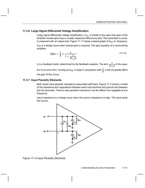
- Page 185 and 186: Additional Parameter Information 11
- Page 187 and 188: Additional Parameter Information +V
- Page 189 and 190: Additional Parameter Information of
- Page 191 and 192: Additional Parameter Information 12
- Page 193 and 194: Chapter 12 Instrumentation: Sensors
- Page 195 and 196: The system definition specifies the
- Page 197 and 198: pends heavily on test conditions su
- Page 199 and 200: the bias resistor, R 1 , is selecte
- Page 201 and 202: V OUT I D R F (12-6) The phototran
- Page 203 and 204: the semiconductor in a direction pe
- Page 205 and 206: eference has a temperature drift of
- Page 207 and 208: impedance of the transducer. The te
- Page 209 and 210: Y mX b (12-14) Two pairs of data
- Page 211 and 212: Table 12-5. Offset and Gain Error B
- Page 213 and 214: R G 23.7 kΩ R FB 280 kΩ R FA 200
- Page 215 and 216: 12.10 Test The final circuit is rea
- Page 217 and 218: Chapter 13 Wireless Communication:
- Page 219 and 220: Wireless Systems ality. Image rejec
- Page 221 and 222: Wireless Systems of the DAC, is usu
- Page 223 and 224: Selection of ADCs/DACs The mean squ
- Page 225 and 226: Selection of ADCs/DACs fication. Wi
- Page 227 and 228: Anti-Aliasing Filters The op amp dy
- Page 229 and 230: Communication D/A Converter Reconst
- Page 231 and 232: External Vref Circuits for ADCs/DAC
- Page 233 and 234:
External Vref Circuits for ADCs/DAC
- Page 235 and 236:
High-Speed Analog Input Drive Circu
- Page 237 and 238:
High-Speed Analog Input Drive Circu
- Page 239 and 240:
Chapter 14 Interfacing D/A Converte
- Page 241 and 242:
Understanding the D/A Converter and
- Page 243 and 244:
Understanding the D/A Converter and
- Page 245 and 246:
D/A Converter Error Budget 14.4.1 A
- Page 247 and 248:
D/A Converter Error Budget 20 Ampli
- Page 249 and 250:
D/A Converter Errors and Parameters
- Page 251 and 252:
D/A Converter Errors and Parameters
- Page 253 and 254:
D/A Converter Errors and Parameters
- Page 255 and 256:
D/A Converter Errors and Parameters
- Page 257 and 258:
Increasing Op Amp Buffer Amplifier
- Page 259 and 260:
Increasing Op Amp Buffer Amplifier
- Page 261 and 262:
Increasing Op Amp Buffer Amplifier
- Page 263 and 264:
Chapter 15 Sine Wave Oscillators Ro
- Page 265 and 266:
Phase Shift in the Oscillator 15.3
- Page 267 and 268:
Active Element (Op Amp) Impact on t
- Page 269 and 270:
Analysis of the Oscillator Operatio
- Page 271 and 272:
Sine Wave Oscillator Circuits Phase
- Page 273 and 274:
Sine Wave Oscillator Circuits large
- Page 275 and 276:
Sine Wave Oscillator Circuits The i
- Page 277 and 278:
Sine Wave Oscillator Circuits R F 1
- Page 279 and 280:
Sine Wave Oscillator Circuits V OUT
- Page 281 and 282:
Sine Wave Oscillator Circuits resis
- Page 283 and 284:
Sine Wave Oscillator Circuits 15.7.
- Page 285 and 286:
Chapter 16 Active Filter Design Tec
- Page 287 and 288:
Fundamentals of Low-Pass Filters V
- Page 289 and 290:
Fundamentals of Low-Pass Filters A(
- Page 291 and 292:
Fundamentals of Low-Pass Filters 16
- Page 293 and 294:
Fundamentals of Low-Pass Filters 10
- Page 295 and 296:
Low-Pass Filter Design The multipli
- Page 297 and 298:
Low-Pass Filter Design C 1 R 1 R 2
- Page 299 and 300:
Low-Pass Filter Design V IN R 1 R 2
- Page 301 and 302:
Low-Pass Filter Design The general
- Page 303 and 304:
Low-Pass Filter Design In order to
- Page 305 and 306:
High-Pass Filter Design With C 1 =
- Page 307 and 308:
High-Pass Filter Design 16.4.1 Firs
- Page 309 and 310:
High-Pass Filter Design To simplify
- Page 311 and 312:
Band-Pass Filter Design R 1 1 1 2
- Page 313 and 314:
Band-Pass Filter Design 16.5.1 Seco
- Page 315 and 316:
Band-Pass Filter Design Because of
- Page 317 and 318:
Band-Pass Filter Design A mi is
- Page 319 and 320:
Band-Pass Filter Design In accordan
- Page 321 and 322:
Band-Rejection Filter Design |A| [d
- Page 323 and 324:
Band-Rejection Filter Design or to
- Page 325 and 326:
All-Pass Filter Design 0 |A| — Ga
- Page 327 and 328:
All-Pass Filter Design Inserting th
- Page 329 and 330:
All-Pass Filter Design The transfer
- Page 331 and 332:
Practical Design Hints 16.8 Practic
- Page 333 and 334:
Practical Design Hints +V CC +V CC
- Page 335 and 336:
Practical Design Hints The differen
- Page 337 and 338:
Practical Design Hints 16.8.4 Op Am
- Page 339 and 340:
Filter Coefficient Tables 16.9 Filt
- Page 341 and 342:
Filter Coefficient Tables Table 16-
- Page 343 and 344:
Filter Coefficient Tables Table 16-
- Page 345 and 346:
Filter Coefficient Tables Table 16-
- Page 347 and 348:
References 16.10 References D.Johns
- Page 349 and 350:
Chapter 17 Circuit Board Layout Tec
- Page 351 and 352:
PCB Mechanical Construction 17.2 PC
- Page 353 and 354:
PCB Mechanical Construction V+ IN -
- Page 355 and 356:
Grounding ponents and feed-throughs
- Page 357 and 358:
Grounding components carefully if t
- Page 359 and 360:
The Frequency Characteristics of Pa
- Page 361 and 362:
The Frequency Characteristics of Pa
- Page 363 and 364:
The Frequency Characteristics of Pa
- Page 365 and 366:
The Frequency Characteristics of Pa
- Page 367 and 368:
The Frequency Characteristics of Pa
- Page 369 and 370:
Decoupling + Figure 17-15. Logic Ga
- Page 371 and 372:
Input and Output Isolation A decoup
- Page 373 and 374:
Packages SINGLE DUAL SHORT TRACES L
- Page 375 and 376:
Packages and other passive componen
- Page 377 and 378:
References 17.8.4 Routing 17.
- Page 379 and 380:
Chapter 18 Designing Low-Voltage Op
- Page 381 and 382:
Dynamic Range The trick to designin
- Page 383 and 384:
Signal-to-Noise Ratio Table 18-1. C
- Page 385 and 386:
Input Common-Mode Range Many low vo
- Page 387 and 388:
Input Common-Mode Range The input s
- Page 389 and 390:
Output Voltage Swing Op amps always
- Page 391 and 392:
Single-Supply Circuit Design every
- Page 393 and 394:
Transducer to ADC Analog Interface
- Page 395 and 396:
DAC to Actuator Analog Interface is
- Page 397 and 398:
DAC to Actuator Analog Interface Th
- Page 399 and 400:
Comparison of Op Amps Table 18-2. O
- Page 401 and 402:
Summary mon-mode range of the op am
- Page 403 and 404:
Appendix A Single-Supply Circuit Co
- Page 405 and 406:
Introduction + 5 V R G R F +V CC _
- Page 407 and 408:
Amplifiers A.3 Amplifiers Many type
- Page 409 and 410:
Amplifiers A.3.3 Inverting Op Amp w
- Page 411 and 412:
Amplifiers A.3.5 Noninverting Op Am
- Page 413 and 414:
Amplifiers A.3.7 Noninverting Op Am
- Page 415 and 416:
Amplifiers A.3.9 Differential Ampli
- Page 417 and 418:
Amplifiers A.3.11 High Input Impeda
- Page 419 and 420:
Amplifiers A.3.13 High-Precision Di
- Page 421 and 422:
Amplifiers A.3.15 Variable Gain Dif
- Page 423 and 424:
Amplifiers A.3.17 Buffer The buffer
- Page 425 and 426:
Amplifiers A.3.19 Noninverting AC A
- Page 427 and 428:
Computing Circuits A.4.2 Noninverti
- Page 429 and 430:
Computing Circuits A.4.4 Inverting
- Page 431 and 432:
Computing Circuits A.4.6 Inverting
- Page 433 and 434:
Computing Circuits A.4.8 Inverting
- Page 435 and 436:
Computing Circuits A.4.10 Noninvert
- Page 437 and 438:
Computing Circuits A.4.12 Inverting
- Page 439 and 440:
Oscillators A.5 Oscillators This se
- Page 441 and 442:
Oscillators A.5.3 Wien Bridge Oscil
- Page 443 and 444:
Oscillators A.5.5 Classical Phase S
- Page 445 and 446:
Oscillators A.5.7 Bubba Oscillator
- Page 447 and 448:
Appendix BA Single-Supply Op Amp Se
- Page 449 and 450:
Table B-1. Single-Supply Operationa
- Page 451 and 452:
A AC loads, DAC, 14-2 AC parameters
- Page 453 and 454:
low pass filter, 16-1 low-pass filt
- Page 455 and 456:
esistor ladder, 14-2 to 14-4 resist
- Page 457 and 458:
phase shift for TL07x, 7-5 phase sh
- Page 459 and 460:
N Noise, 10-8 to 10-10 avalanche, 1
- Page 461 and 462:
packages, 17-24 to 17-27 parallel s
- Page 463 and 464:
Theorem Norton’s, 2-5 Superpositi