RTL8181 Wireless LAN Access Point/Gateway Controller DATA ...
RTL8181 Wireless LAN Access Point/Gateway Controller DATA ...
RTL8181 Wireless LAN Access Point/Gateway Controller DATA ...
- No tags were found...

You also want an ePaper? Increase the reach of your titles
YUMPU automatically turns print PDFs into web optimized ePapers that Google loves.
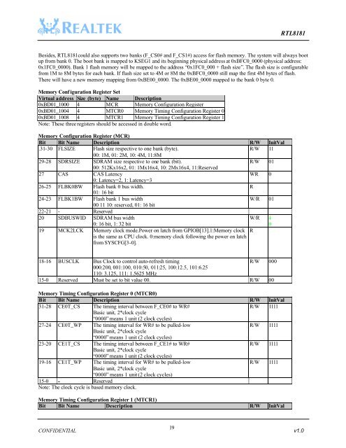
<strong>RTL8181</strong>Besides, <strong>RTL8181</strong>could also supports two banks (F_CS0# and F_CS1#) access for flash memory. The system will always bootup from bank 0. The boot bank is mapped to KSEG1 and its beginning physical address at 0xBFC0_0000 (physical address:0x1FC0_0000). Bank 1 flash memory will be mapped to the address “0x1FC0_000 + flash size”. The flash size is configurablefrom 1M to 8M bytes for each bank. If flash size set to 4M or 8M the 0xBFC0_0000 still map the first 4M bytes of flash.There will have a new memory mapping from 0xBE00_0000. The 0xBE00_0000 mapped to the bank 0 byte 0.Memory Conf iguration Register SetVirtual address Size (byte) Name Description0xBD01_1000 4 MCR Memory Configuration Register0xBD01_1004 4 MTCR0 Memory Timing Configuration Register 00xBD01_1008 4 MTCR1 Memory Timing Configuration Register 1Note: These three registers should be accessed in double word.Memory Configuration Register (MCR)Bit Bit Name Description R/W InitVal.31-30 FLSIZE Flash size respective to one bank (byte).R/W 1100: 1M, 01: 2M, 10: 4M, 11:8M29-28 SDRSIZE SDRAM size respective to one bank (bit).R/W 0100: 512Kx16x2, 01: 1Mx16x4, 10: 2Mx16x4, 11:Reserved27 CAS CAS LatencyWR 00: Latency=2, 1: Latency=326-25 FLBK0BW Flash bank 0 bus width.R01: 16 bit24-23 FLBK1BW Flash bank 1 bus widthW/R 0100 11 10: reserved, 01: 16 bit22-21 - Reserved20 SDBUSWID SDRAM bus width0: 16 bit, 1: 32 bitW/R 1019 MCK2LCK Memory clock mode.Power on latch from GPIOB[13].1:Memory clockis the same as CPU clock. 0:memory clock following the power on latchfrom SYSCFG[3-0].R18-16 BUSCLK Bus Clock to control auto-refresh timingR/W 000000:200, 001:100, 010:50, 011:25, 100:12.5, 101:6.25110: 3.125, 111: 1.5625 MHz15-0 Reserved Must be set to bit value 00. R/W 00Memory Timing Configuration Register 0 (MTCR0)Bit Bit Name Description R/W InitVal31-28 CE0T_CS The timing interval between F_CE0# to WR#R/W 1111Basic unit, 2*clock cycle“0000” means 1 unit (2 clock cycles)27-24 CE0T_WP The timing interval for WR# to be pulled-lowR/W 1111Basic unit, 2*clock cycle“0000” means 1 unit (2 clock cycles)23-20 CE1T_CS The timing interval between F_CE1# to WR#R/W 1111Basic unit, 2*clock cycle“0000” means 1 unit (2 clock cycles)19-16 CE1T_WP The timing interval for WR# to be pulled-lowR/W 1111Basic unit, 2*clock cycle“0000” means 1 unit (2 clock cycles)15-0 - ReservedNote: The clock cycle is based memory clock.Memory Timing Configuration Register 1 (MTCR1)Bit Bit Name Description R/W InitVal19CONFIDENTIAL v1.0