RTL8181 Wireless LAN Access Point/Gateway Controller DATA ...
RTL8181 Wireless LAN Access Point/Gateway Controller DATA ...
RTL8181 Wireless LAN Access Point/Gateway Controller DATA ...
- No tags were found...

Create successful ePaper yourself
Turn your PDF publications into a flip-book with our unique Google optimized e-Paper software.
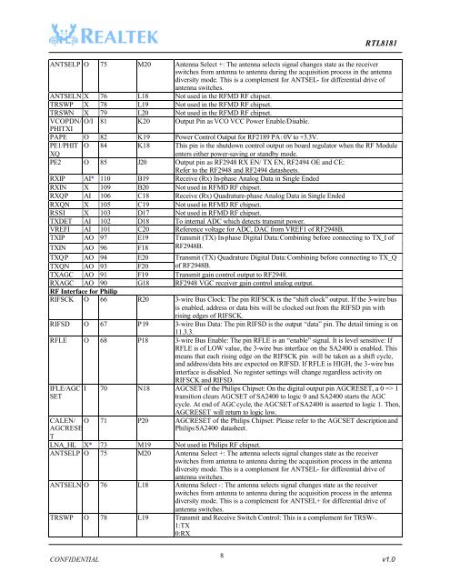
<strong>RTL8181</strong>ANTSELP O 75 M20 Antenna Select +: The antenna selects signal changes state as the receiverswitches from antenna to antenna during the acquisition process in the antennadiversity mode. This is a complement for ANTSEL- for differential drive ofantenna switches.ANTSELN X 76 L18 Not used in the RFMD RF chipset.TRSWP X 78 L19 Not used in the RFMD RF chipset.TRSWN X 79 L20 Not used in the RFMD RF chipset.VCOPDN/ O/I 81 K20 Output Pin as VCO VCC Power Enable/Disable.PHITXIPAPE O 82 K19 Power Control Output for RF2189 PA: 0V to +3.3V.PE1/PHIT O 84 K18 This pin is the shutdown control output on board regulator when the RF ModuleXQenters either power-saving or standby mode.PE2 O 85 J20 Output pin as RF2948 RX EN/ TX EN, RF2494 OE and CE:Refer to the RF2948 and RF2494 datasheets.RXIP AI* 110 B19 Receive (Rx) In-phase Analog Data in Single EndedRXIN X 109 B20 Not used in RFMD RF chipset.RXQP AI 106 C18 Receive (Rx) Quadrature-phase Analog Data in Single EndedRXQN X 105 C19 Not used in RFMD RF chipset.RSSI X 103 D17 Not used in RFMD RF chipset.TXDET AI 102 D18 To internal ADC which detects transmit power.VREFI AI 101 C20 Reference voltage for ADC, DAC from VREF1 of RF2948B.TXIP AO 97 E19 Transmit (TX) In-phase Digital Data: Combining before connecting to TX_I ofTXIN AO 96 F18 RF2948B.TXQP AO 94 E20 Transmit (TX) Quadrature Digital Data: Combining before connecting to TX_QTXQN AO 93 F20 of RF2948B.TXAGC AO 91 F19 Transmit gain control output to RF2948.RXAGC AO 90 G18 RF2948 VGC receiver gain control analog output.RF Interface for PhilipRIFSCK O 66 R20 3-wire Bus Clock: The pin RIFSCK is the “shift clock” output. If the 3-wire busis enabled, address or data bits will be clocked out from the RIFSD pin withrising edges of RIFSCK.RIFSD O 67 P19 3-wire Bus Data: The pin RIFSD is the output “data” pin. The detail timing is on11.3.3.RFLE O 68 P18 3-wire Bus Enable: The pin RFLE is an “enable” signal. It is level sensitive: IfRFLE is of LOW value, the 3-wire bus interface on the SA2400 is enabled. Thismeans that each rising edge on the RIFSCK pin will be taken as a shift cycle,and address/data bits are expected on RIFSD. If RFLE is HIGH, the 3-wire businterface is disabled. No register settings will change regardless activity onRIFSCK and RIFSD.IFLE/AGCSETI 70 N18 AGCSET of the Philips Chipset: On the digital output pin AGCRESET, a 0 => 1transition clears AGCSET of SA2400 to logic 0 and SA2400 starts the AGCcycle. At end of AGC cycle, the AGCSET of SA2400 is asserted to logic 1. Then,AGCRESET will return to logic low.CALEN/AGCRESEO 71 P20 AGCRESET of the Philips Chipset: Please refer to the AGCSET description andPhilips SA2400 datasheet.TLNA_HL X* 73 M19 Not used in Philips RF chipset.ANTSELP O 75 M20 Antenna Select +: The antenna selects signal changes state as the receiverswitches from antenna to antenna during the acquisition process in the antennadiversity mode. This is a complement for ANTSEL- for differential drive ofantenna switches.ANTSELN O 76 L18 Antenna Select -: The antenna selects signal changes state as the receiverswitches from antenna to antenna during the acquisition process in the antennadiversity mode. This is a complement for ANTSEL+ for differential drive ofantenna switches.TRSWP O 78 L19 Transmit and Receive Switch Control: This is a complement for TRSW-.1:TX0:RX8CONFIDENTIAL v1.0