PICAXE Manual Section 1 - TechnoPujades - Free
PICAXE Manual Section 1 - TechnoPujades - Free
PICAXE Manual Section 1 - TechnoPujades - Free
- No tags were found...

Create successful ePaper yourself
Turn your PDF publications into a flip-book with our unique Google optimized e-Paper software.
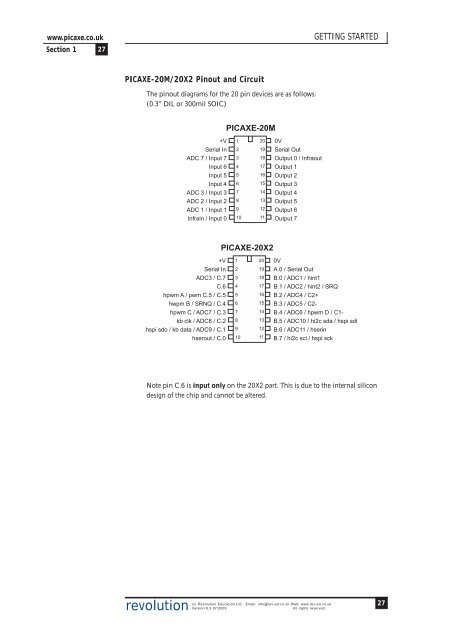
www.picaxe.co.uk<strong>Section</strong> 1 27GETTING STARTED<strong>PICAXE</strong>-20M/20X2 Pinout and CircuitThe pinout diagrams for the 20 pin devices are as follows:(0.3” DIL or 300mil SOIC)<strong>PICAXE</strong>-20M+VSerial InADC 7 / Input 7Input 6Input 5Input 4ADC 3 / Input 3ADC 2 / Input 2ADC 1 / Input 1Infrain / Input 012345678910201918171615141312110VSerial OutOutput 0 / InfraoutOutput 1Output 2Output 3Output 4Output 5Output 6Output 7<strong>PICAXE</strong>-20X2+VSerial InADC3 / C.7C.6hpwm A / pwm C.5 / C.5hwpm B / SRNQ / C.4hpwm C / ADC7 / C.3kb clk / ADC8 / C.2hspi sdo / kb data / ADC9 / C.1hserout / C.012345678910201918171615141312110VA.0 / Serial OutB.0 / ADC1 / hint1B.1 / ADC2 / hint2 / SRQB.2 / ADC4 / C2+B.3 / ADC5 / C2-B.4 / ADC6 / hpwm D / C1-B.5 / ADC10 / hi2c sda / hspi sdiB.6 / ADC11 / hserinB.7 / hi2c scl / hspi sckNote pin C.6 is input only on the 20X2 part. This is due to the internal silicondesign of the chip and cannot be altered.revolution(c) Revolution Education Ltd. Email: info@rev-ed.co.uk Web: www.rev-ed.co.ukVersion 6.9 07/2009All rights reserved.27