PICAXE Manual Section 1 - TechnoPujades - Free
PICAXE Manual Section 1 - TechnoPujades - Free
PICAXE Manual Section 1 - TechnoPujades - Free
- No tags were found...

Create successful ePaper yourself
Turn your PDF publications into a flip-book with our unique Google optimized e-Paper software.
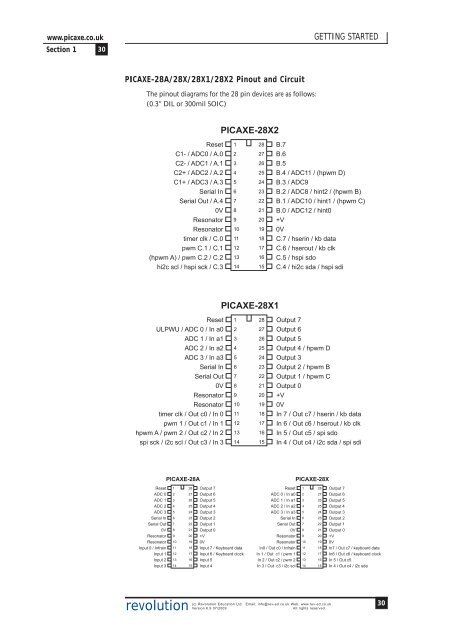
www.picaxe.co.uk<strong>Section</strong> 1 30GETTING STARTED<strong>PICAXE</strong>-28A/28X/28X1/28X2 Pinout and CircuitThe pinout diagrams for the 28 pin devices are as follows:(0.3” DIL or 300mil SOIC)<strong>PICAXE</strong>-28X2ResetC1- / ADC0 / A.0C2- / ADC1 / A.1C2+ / ADC2 / A.2C1+ / ADC3 / A.3Serial InSerial Out / A.40VResonatorResonatortimer clk / C.0pwm C.1 / C.1(hpwm A) / pwm C.2 / C.2hi2c scl / hspi sck / C.312345678910111213142827262524232221201918171615B.7B.6B.5B.4 / ADC11 / (hpwm D)B.3 / ADC9B.2 / ADC8 / hint2 / (hpwm B)B.1 / ADC10 / hint1 / (hpwm C)B.0 / ADC12 / hint0+V0VC.7 / hserin / kb dataC.6 / hserout / kb clkC.5 / hspi sdoC.4 / hi2c sda / hspi sdi<strong>PICAXE</strong>-28X1ResetULPWU / ADC 0 / In a0ADC 1 / In a1ADC 2 / In a2ADC 3 / In a3Serial InSerial Out0VResonatorResonatortimer clk / Out c0 / In 0pwm 1 / Out c1 / In 1hpwm A / pwm 2 / Out c2 / In 2spi sck / i2c scl / Out c3 / In 312345678910111213142827262524232221201918171615Output 7Output 6Output 5Output 4 / hpwm DOutput 3Output 2 / hpwm BOutput 1 / hpwm COutput 0+V0VIn 7 / Out c7 / hserin / kb dataIn 6 / Out c6 / hserout / kb clkIn 5 / Out c5 / spi sdoIn 4 / Out c4 / i2c sda / spi sdiResetADC 0ADC 1ADC 2ADC 3Serial InSerial Out0VResonatorResonatorInput 0 / InfrainInput 1Input 2Input 3<strong>PICAXE</strong>-28A12345678910111213142827262524232221201918171615Output 7Output 6Output 5Output 4Output 3Output 2Output 1Output 0+V0VInput 7 / Keyboard dataInput 6 / Keyboard clockInput 5Input 4ResetADC 0 / In a0ADC 1 / In a1ADC 2 / In a2ADC 3 / In a3Serial InSerial Out0VResonatorResonatorIn0 / Out c0 / InfrainIn 1 / Out c1 / pwm 1In 2 / Out c2 / pwm 2In 3 / Out c3 / i2c scl<strong>PICAXE</strong>-28X12345678910111213142827262524232221201918171615Output 7Output 6Output 5Output 4Output 3Output 2Output 1Output 0+V0VIn7 / Out c7 / keyboard dataIn6 / Out c6 / keyboard clockIn 5 / Out c5In 4 / Out c4 / i2c sdarevolution(c) Revolution Education Ltd. Email: info@rev-ed.co.uk Web: www.rev-ed.co.ukVersion 6.9 07/2009All rights reserved.30