Abstract Download (8.38MB)
Abstract Download (8.38MB)
Abstract Download (8.38MB)

You also want an ePaper? Increase the reach of your titles
YUMPU automatically turns print PDFs into web optimized ePapers that Google loves.
Name (Title):<br />
Jun Chen (ICYS-MANA Researcher)<br />
Affiliation:<br />
International Center for Young Scientists (ICYS) &<br />
International Center for Materials Nanoarchitechtonics (MANA), NIMS<br />
Address:<br />
1-1 Namiki, Tsukuba, Ibaraki 305-0044, Japan<br />
Email: CHEN.Jun@nims.go.jp<br />
Home Page:<br />
Presentation Title:<br />
A versatile application of electron-beam-induced current technique in semiconductor diagnosis<br />
<strong>Abstract</strong>:<br />
We presented advanced semiconductor diagnosis by using electron-beam-induced current<br />
(EBIC) technique. By varying the parameters such as temperature, accelerating voltage, bias<br />
voltage, and time, it is possible to extend EBIC application from conventional defect<br />
characterization to advanced device diagnosis. Since electron beam can excite a certain volume<br />
even it is beneath the surface passive layer, EBIC can sometimes very easy to diagnose<br />
complicated devices with hybrid structure.<br />
Three topics were selected to demonstrate EBIC applications.[1] First, the electrical<br />
recombination activities of grain boundaries and their interaction with Fe impurity in<br />
photovoltaic multicrystalline Si are clarified by temperature-dependent EBIC. Second, the<br />
detection of dislocations between strained-Si and SiGe virtual substrate are shown to overcome<br />
the limitation of depletion region. Third, the observation of leakage sites in high-k gate dielectric<br />
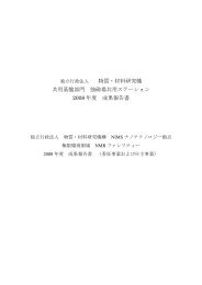
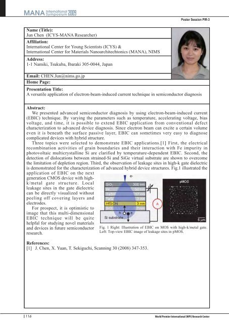
is demonstrated for the characterization of advanced hybrid device structures. Fig.1 illustrated the<br />
application of EBIC on the next<br />
generation CMOS device with highk/metal<br />
gate structure. Local<br />
leakage sites in the gate dielectric<br />
can be directly visualized without<br />
peeling off covering layers and<br />
electrodes.<br />
For prospect, it is optimistic to<br />
image that this multi-dimensional<br />
EBIC technique will be quite<br />
helpful for studying novel materials<br />
and devices in future semiconductor<br />
research.<br />
References:<br />
[1] J. Chen, X. Yuan, T. Sekiguchi, Scanning 30 (2008) 347-353.<br />
116<br />
Poster Session PIR-3<br />
Fig. 1 Right: Illustration of EBIC on MOS with high-k/metal gate.<br />
Left: Top-view EBIC image of leakage sites in pMOS.