Abstract Download (8.38MB)
Abstract Download (8.38MB)
Abstract Download (8.38MB)

Create successful ePaper yourself
Turn your PDF publications into a flip-book with our unique Google optimized e-Paper software.
Name (Title):<br />
Makoto Sakurai (MANA scientist)<br />
Affiliation:<br />
International Center for Materials Nanoarchitectronics<br />
(MANA), NIMS<br />
Address:<br />
1-1 Namiki, Tsukuba, Ibaraki 305-0044, Japan<br />
Email: SAKURAI.Makoto@nims.go.jp<br />
Home Page:<br />
Presentation Title:<br />
Fabrication and characterization of individual ZnO nanowires<br />
<strong>Abstract</strong>:<br />
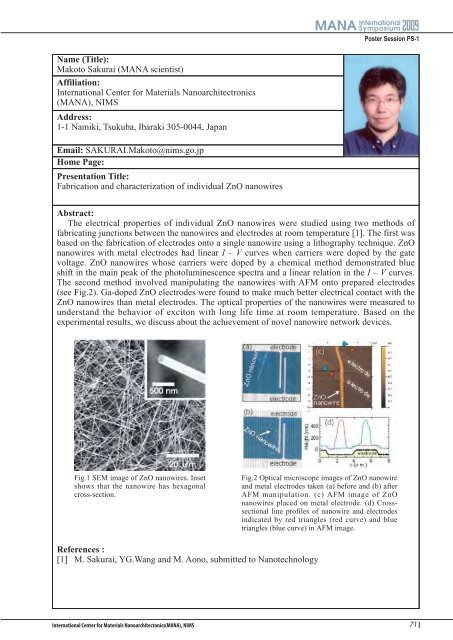
The electrical properties of individual ZnO nanowires were studied using two methods of<br />
fabricating junctions between the nanowires and electrodes at room temperature [1]. The first was<br />
based on the fabrication of electrodes onto a single nanowire using a lithography technique. ZnO<br />
nanowires with metal electrodes had linear I – V curves when carriers were doped by the gate<br />
voltage. ZnO nanowires whose carriers were doped by a chemical method demonstrated blue<br />
shift in the main peak of the photoluminescence spectra and a linear relation in the I – V curves.<br />
The second method involved manipulating the nanowires with AFM onto prepared electrodes<br />
(see Fig.2). Ga-doped ZnO electrodes were found to make much better electrical contact with the<br />
ZnO nanowires than metal electrodes. The optical properties of the nanowires were measured to<br />
understand the behavior of exciton with long life time at room temperature. Based on the<br />
experimental results, we discuss about the achievement of novel nanowire network devices.<br />
Fig.1 SEM image of ZnO nanowires. Inset<br />
shows that the nanowire has hexagonal<br />
cross-section.<br />
References :<br />
[1] M. Sakurai, YG.Wang and M. Aono, submitted to Nanotechnology<br />
Poster Session PS-1<br />
Fig.2 Optical microscope images of ZnO nanowire<br />
and metal electrodes taken (a) before and (b) after<br />
AFM manipulation. (c) AFM image of ZnO<br />
nanowires placed on metal electrode. (d) Crosssectional<br />
line profiles of nanowire and electrodes<br />
indicated by red triangles (red curve) and blue<br />
triangles (blue curve) in AFM image.<br />
71