Abstract Download (8.38MB)
Abstract Download (8.38MB)
Abstract Download (8.38MB)

Create successful ePaper yourself
Turn your PDF publications into a flip-book with our unique Google optimized e-Paper software.
Name (Title):<br />
Canhua Liu (ICYS-MANA researcher)<br />
Affiliation:<br />
International Center for Young Scientists<br />
(MANA), NIMS<br />
Address:<br />
1-1 Namiki, Tsukuba, Ibaraki 305-0875, Japan<br />
Email: liu.canhua@nims.go.jp<br />
Home Page: http://www.nims.go.jp/mana/members/icys_mana_researcher/c_liu<br />
Presentation Title:<br />
Phase modulation of quasi-one-dimensional charge-density waves induced by impurities<br />
<strong>Abstract</strong>:<br />
Low-dimensional materials<br />
attract strong research interests<br />
because of their fascinating<br />
properties due to size reduction<br />
and their promising for future<br />
applications. Being cooled to a<br />
critical temperature, pure lowdimensional<br />
metals generally<br />
undergo a Peierls transition,<br />
which leads to the formation of<br />
charge-density waves (CDW)<br />
accompanied by a periodic<br />
lattice distortion through<br />
electron- phonon coupling.<br />
Impurities play an important<br />
part in determining both static<br />
and dynamic CDW properties<br />
through scattering electrons,<br />
which modifies both phase and<br />
amplitude of the CDW state. Especially, the phase pinning of CDW due to interaction with<br />
impurities is a central concept for explaining various phenomena including nonlinear conductivity<br />
and narrow band noise [1]. This issue, however, remains to be fully understood in spite of<br />
enormous theoretical and experimental studies, partly because of the absence of direct observation<br />
of the phase modulation in real space.<br />
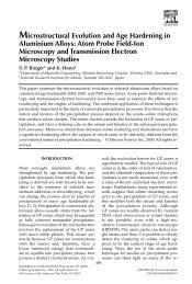
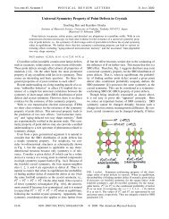
A self-organized array of In atomic wires, the Si(111)-4x1-In surface, provides the opportunity<br />
of such direct observation as it exhibits the quasi-one-dimensional (Q1D) CDW transition [2,3],<br />
as long as scanning tunneling microscopy (STM) is applied. By adding very small amount of Co<br />
adsorbates (~0.02 ML) onto the In atomic wires and with STM performed at 80 K, we succeeded<br />
in obtaining direct images of the phase and amplitude modulation of CDW due to the emergence<br />
of Co adatoms. Concepts of phase pinning, phase slip and phase fluctuation are used to interpret<br />
the observed phase modulation that shows a strong bias dependence. Our observation discovers<br />
some new defect effects on the CDW that have not been reported yet.<br />
References:<br />
[1] G. Grüner, Rev. Mod. Phys. 60, 1129 (1988).<br />
[2] H. W. Yeom, et al., Phys. Rev. Lett. 82, 4898 (1999).<br />
[3] C. Liu, T. Uchihashi, and T. Nakayama, Phys. Rev. Lett. 101, 145104 (2008).<br />
Poster Session PIR-6<br />
Fig. (a) STM image of Co adatoms (bright protrusions) adsorbed Si(111)-<br />
4x1-In surface taken at -1.2 V. (b) Line profiles taken of the lines indicated<br />
in (a), showing CDW phase modulations as arrows indicate.<br />
119