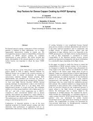
Abstract Download (8.38MB)
Abstract Download (8.38MB)
Abstract Download (8.38MB)

Create successful ePaper yourself
Turn your PDF publications into a flip-book with our unique Google optimized e-Paper software.
Name (Title):<br />
Baodan Liu (NIMS Postdoc)<br />
Affiliation:<br />
International Center for Materials Nanoarchitectonics, (MANA), NIMS<br />
Address:<br />
1-1 Namiki, Tsukuba. Ibaraki 305-0044, Japan<br />
Email: baodanliu@gmail.com<br />
Home Page: http://www.nims.go.jp/mana/<br />
Presentation Title:<br />
Compositional design, structural analysis and property studies of one-dimensional (1D) wide<br />
band-gap semiconductor nanostructures<br />
<strong>Abstract</strong>:<br />
Here we demonstrate that diverse nanostructures including (needle-like) nanowires,<br />
(bicrystalline) nanobelts, nanotubes, nanocones and other novel architectures made of various<br />
wide band-gap semiconductors, e.g. GaN, ZnS, AlN, GaP, SiC and so forth can be fabricated<br />
through a well-designed and carefully controlled chemical vapor deposition (CVD). The<br />
nanostructures growth was promoted by a catalyst particle attached to their tips, and the vaporliquid-solid<br />
(V-L-S) growth mechanism thus became in effect. The size, morphology,<br />
crystallinity, phase composition,<br />
purity, and properties of the<br />
nanomaterials were delicately<br />
tuned through an experimental<br />
conditions control. Moreover, some<br />
complex nanostructures can also be<br />
fabricated for specific applications.<br />
Analyses of crystallography,<br />
phases, and constituents of these<br />
novel nanostructures were carried<br />
out by means of a 300-kV<br />
transmission electron microscope<br />
(TEM) equipped with an energy<br />
dispersive X-ray spectrometer<br />
(EDS) and an electron energy loss<br />
(EELS) spectrometer. Optical and<br />
electrical measurements on the<br />
present nano-semiconductors<br />
indicated that they exhibit potential<br />
applications in novel nano-<br />
optoelectronic devices, field<br />
emission transistors (FET) and<br />
sensors with a tunable working<br />
wavelength, i.e. from ultraviolet<br />
(UV) to a visible light.<br />
References:<br />
[1] B. D. Liu et al, J. Phys. Chem. B, 109, (2005) 10782.<br />
Poster Session PM-3<br />
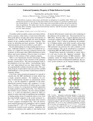
Fig. (a) Low magnification TEM image; (b) HRTEM image and (c)<br />
corresponding electron diffraction (ED) patterns of a bicrystalline ZnS<br />
nanobelt.<br />
45