Abstract Download (8.38MB)
Abstract Download (8.38MB)
Abstract Download (8.38MB)

Create successful ePaper yourself
Turn your PDF publications into a flip-book with our unique Google optimized e-Paper software.
Name (Title):<br />
Masataka Imura (ICYS-MANA)<br />
Affiliation:<br />
International Center for Materials Nanoarchitectonics<br />
Address:<br />
1-1 Namiki, Tsukuba. Ibaraki 305-0044, Japan<br />
Email: IMURA.Masataka@nims.go.jp<br />
Home Page:<br />
Presentation Title:<br />
Deep-ultraviolet Diamond-based Photodetector for high-power excimer lamp<br />
<strong>Abstract</strong>:<br />
The next generation photolithography system, which uses a stepper with an excimer laser such<br />
as an ArF laser (λ=193nm) and an F2 laser (λ=157nm), requires deep-ultraviolet (DUV) detection.<br />
Currently, Si-based photodetectors are primarily used to detect UV light. However, they require<br />
filters to stop energy photons from visible and infrared light and have low efficiency. In addition,<br />
they easily degrade by the UV light. Diamond-based photodetector is a promising candidate for<br />
UV and DUV detection and overcome these limitations. In order to achieve and demonstrate<br />
diamond-based photodetector for UV and DUV detection, we fabricated Schottky barrier<br />
photodiode (SPD) with the vertical-type by using heavily B-doped p + -diamond (100) substrates.<br />
The p-diamond epilayers were homoepitaxially grown by microwave plasma chemical vapor<br />
deposition (MPCVD) on the heavily B-doped p + -diamond (100) substrates commercialized by<br />
Technological Institute for Super-hard and Novel Carbon Materials (TISNCM). The substrate<br />
was 2.5 × 2.5 × 0.5 mm 3 in size, and the B concentration ([B]) was measured to be around 1×10 20<br />
cm -3 by secondary-ion mass spectroscopy (SIMS). The unintentionally B-doped p-diamond<br />
epilayers with [B] in the range 10 15 to 10 16 cm -3 analyzed by SIMS were grown by CH4 and H2<br />
gases. The ratio of CH4 to H2 was 0.08 %, and the corresponding flow rates of CH4 and H2 were<br />
0.4 and 500 sccm, respectively. The reactor pressure was fixed at 106 hPa during growth. The<br />
growth was performed at ~800 °C. The thickness of epilayer was about 0.5 µm. To obtain Ohmic<br />
contact, Ti (40 nm)/ WC (30 nm) films were deposited on the back-side of the diamond substrate,<br />
subsequently annealed at 600 °C for 1 h in an argon ambient. The semitransparent WC Schottky<br />
contact was deposited on the defined circle patterns on the diamond epilayer by a<br />
photolithographic technique. The diameter of WC Schottky<br />
contact was 1 mm.<br />
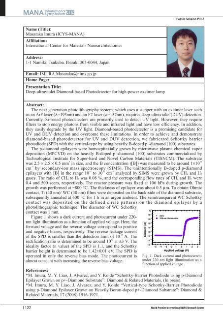
Figure 1 shows a dark current and photocurrent under 220nm<br />
light illumination as a function of applied voltage. Here, the<br />
forward voltage and the reverse voltage correspond to positive<br />
and negative biases, respectively. The reverse leakage current<br />
of the SPD is smaller than the detection limit of 10 -14 A. The<br />
rectification ratio is determined to be around 10 12 at ±3 V. The<br />
ideality factor (n value) of the SPD is 1.1, and the Schottky<br />
barrier height is determined to be 1.42±0.01 eV. The SPD is<br />
operated in only the reverse bias mode. The photocurrent is<br />
almost constant with increasing the reverse bias voltage.<br />
References:<br />
*M. Imura, M. Y. Liao, J. Alvarez, and Y. Koide “Schottky-Barrier Photodiode using p-Diamond<br />
Epilayer Grown on p+-Diamond Substrate”: Diamond & Related Materials, (In press).<br />
*M. Imura, M. Y. Liao, J. Alvarez, and Y. Koide “Vertical-type Schottky-Barrier Photodiode<br />
using p-Diamond Epilayer Grown on Heavily Boron-doped p+-Diamond Substrate”: Diamond &<br />
Related Materials, 17 (2008) 1916-1921.<br />
120<br />
Current (A)<br />
�� �<br />
�� ��<br />
�� ��<br />
�� ��<br />
�� ��<br />
�� ��<br />
�� ���<br />
�� ���<br />
�� ���<br />
dark<br />
220-nm illumination<br />
Poster Session PIR-7<br />
�� �� �� �� �� � � � �<br />
Applied voltage (V)<br />
Fig. 1. Dark current and photocurrent<br />
under 220-nm light illumination as a<br />
function of applied voltage