Hardware Manual - RTD Embedded Technologies, Inc.
Hardware Manual - RTD Embedded Technologies, Inc.
Hardware Manual - RTD Embedded Technologies, Inc.

You also want an ePaper? Increase the reach of your titles
YUMPU automatically turns print PDFs into web optimized ePapers that Google loves.
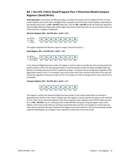
BA + 0x41Ch (1052): Read/Program Port 2 Direction/Mask/Compare<br />
Registers (Read/Write)<br />
8-bit Operation. A read clears the IRQ status flag or provides the contents of one of digital I/O Port 2’s three<br />
control registers; and a write clears the digital chip or programs one of the three control registers, depending on<br />
the setting of bits 0 and 1 at BA + 0x41Eh. When bits 1 and 0 at BA + 0x41Eh are 00, the read/write operations<br />
clear the digital IRQ status flag (read) and the digital chip (write). When these bits are set to any other value, one<br />
of the three Port 2 registers is addressed.<br />
Direction Register (BA + 0x41Eh, bits 1 and 0 = 01):<br />
For all bits:<br />
0 = input<br />
1 = output<br />
D7 D6 D5 D4 D3 D2 D1 D0<br />
P2.7 P2.6 P2.5 P2.4 P2.3 P2.2 P2.1 P2.0<br />
This register programs the direction, input or output, of each bit at Port 2.<br />
Mask Register (BA + 0x41Eh, bits 1 and 0 = 10):<br />
For all bits:<br />
0 = bit enabled<br />
1 = bit masked<br />
D7 D6 D5 D4 D3 D2 D1 D0<br />
P2.7 P2.6 P2.5 P2.4 P2.3 P2.2 P2.1 P2.0<br />
In the Advanced Digital Interrupt modes, this register is used to mask out specific bits when monitoring the bit<br />
pattern present at Port 2 for interrupt generation. In normal operation where the Advanced Digital Interrupt<br />
feature is not being used, any bit which is masked by writing a 1 to that bit will not change state, regardless of the<br />
digital data written to Port 2. For example, if you set the state of bit 0 low and then mask this bit, the state will<br />
remain low, regardless of what you output at Port 2 (an output of 1 will not change the bit’s state until the bit is<br />
unmasked).<br />
Compare Register (BA + 0x41Eh, bits 1 and 0 = 11):<br />
D7 D6 D5 D4 D3 D2 D1 D0<br />
P2.7 P2.6 P2.5 P2.4 P2.3 P2.2 P2.1 P2.0<br />
This register is used for the Advanced Digital Interrupt modes. In the match mode where an interrupt is<br />
generated when the Port 2 bits match a loaded value, this register is used to load the bit pattern to be matched<br />
at Port 2. Bits can be selectively masked so that they are ignored when making a match. NOTE: Make sure that<br />
bit 3 at BA + 0x41Eh is set to 1, selecting match mode, BEFORE writing the Compare Register value at this<br />
address. In the event mode where an interrupt is generated when any Port 2 bit changes its current state, the<br />
value which caused the interrupt is latched at this register and can be read from it. Bits can be selectively masked<br />
using the Mask Register so a change of state is ignored on these lines in the event mode.<br />
BDM-610010034 Rev C Chapter 4: I/O Mapping 55