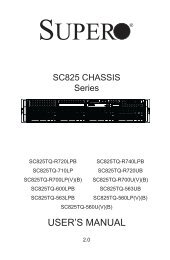
X9DR3_i-LN4F+ 1.1.indb - Supermicro
X9DR3_i-LN4F+ 1.1.indb - Supermicro
X9DR3_i-LN4F+ 1.1.indb - Supermicro

Create successful ePaper yourself
Turn your PDF publications into a flip-book with our unique Google optimized e-Paper software.
J21<br />
JL1<br />
J17<br />
JI2C2<br />
JI2C1<br />
J18<br />
LEM1<br />
SAS4~7<br />
JWP1<br />
SAS0~3<br />
1<br />
XDP-CPU<br />
JD1<br />
JP7<br />
JP6<br />
JF2<br />
1<br />
LE2<br />
SW1<br />
UID<br />
VGA<br />
JF1<br />
LAN2/4<br />
LE1<br />
LAN1/3 USB 2/3 USB 0/1<br />
IPMI_LAN<br />
COM1<br />
FAN1<br />
<strong>X9DR3</strong>-<strong>LN4F+</strong>/X9DRi-<strong>LN4F+</strong> Motherboard User’s Manual<br />
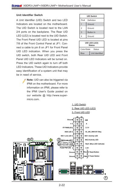
Unit Identifier Switch<br />
A Unit Identifier (UID) Switch and two LED<br />
Indicators are located on the motherboard.<br />
The UID Switch is located next to the LAN<br />
2/4 ports on the backplane. The Rear UID<br />
LED (LE2) is located next to the UID Switch.<br />
The Front Panel UID LED is located at pins<br />
7/8 of the Front Control Panel at JF1. Connect<br />
a cable to pin 8 on JF1 for Front Panel<br />
UID LED indication. When you press the<br />
UID switch, both Rear UID LED and Front<br />
Panel UID LED Indicators will be turned on.<br />
Press the UID switch again to turn off both<br />
LED Indicators. These UID Indicators provide<br />
easy identification of a system unit that may<br />
be in need of service.<br />
Note: UID can also be triggered via<br />
IPMI on the motherboard. For more<br />
information on IPMI, please refer to<br />
the IPMI User's Guide posted on<br />
our website @ http://www.supermicro.com.<br />
Pin#<br />
UID Switch<br />
Definition<br />
1 Ground<br />
2 Ground<br />
3 Button In<br />
4 Ground<br />
UID LED (LE2)<br />
Status<br />
Color/State<br />
Blue<br />
Status<br />
Unit Identified<br />
1. UID Switch<br />
2. Rear UID LED (LE2)<br />
3. Front UID LED<br />
20<br />
19<br />
Ground<br />
NMI<br />
X<br />
X<br />
FP PWRLED<br />
3.3 V<br />
HDD LED<br />
ID_UID_SW/3/3V Stby<br />
JBMC1 JSTBY1<br />
JPG1<br />
JTPM1<br />
COM2<br />
CPU1 Slot1 PCI-E 3.0 x16<br />
SAS<br />
CTRL<br />
BMC<br />
CTRL<br />
CPU1 Slot2 PCI-E 3.0 x4 (in X8 slot)<br />
CPU1 Slot3 PCI-E 3.0 x16<br />
JPB1<br />
CPU2 Slot4 PCI-E 3.0 x16<br />
LAN<br />
CTRL<br />
CPU2 Slot5 PCI-E 3.0 x16<br />
JPL1<br />
2 1<br />
CPU2 Slot6 PCI-E 3.0 x8<br />
P2 DIMMF3<br />
P2 DIMMF2<br />
P2 DIMMF1<br />
P2 DIMME3<br />
P2 DIMME2<br />
P2 DIMME1<br />
Alaways populate DIMMx1 first<br />
CPU2<br />
FAN6<br />
P2 DIMMG1<br />
P2 DIMMG2<br />
P2 DIMMG3<br />
P2 DIMMH1<br />
P2 DIMMH2<br />
P2 DIMMH3<br />
FAN5<br />
PHY<br />
3<br />
NIC1 Link LED<br />
NIC2 Link LED<br />
Blue+ (OH/Fan Fail/<br />
PWR FaiL/UID LED)<br />
Power Fail LED<br />
Ground<br />
Ground<br />
2<br />
1<br />
NIC1 Activity LED<br />
NIC2 Activity LED<br />
Red+ (Blue LED Cathode)<br />
3.3V<br />
Reset Reset Button<br />
PWR Power Button<br />
USB9<br />
JBT1<br />
BIOS BOX<br />
JBAT1<br />
<strong>X9DR3</strong>-<strong>LN4F+</strong>/X9DRi-<strong>LN4F+</strong><br />
Rev. 1.10<br />
JPI2C1<br />
IPMB<br />
JPME2<br />
USB6/7 USB4/5<br />
JWD1<br />
I-SATA4 JPME1<br />
I-SATA2<br />
I-SATA0<br />
I-SATA5<br />
I-SATA3<br />
I-SATA1<br />
JSD1<br />
PCH<br />
XDP-PCH<br />
JRK1<br />
BIOS<br />
FANB<br />
FANA<br />
JOH1<br />
SP1<br />
FAN4<br />
Alaways populate DIMMx1 first<br />
P1 DIMMC1<br />
FAN3<br />
P1 DIMMC3<br />
P1 DIMMC2<br />
P1 DIMMD3<br />
P1 DIMMD2<br />
P1 DIMMD1<br />
CPU1<br />
P1 DIMMA1<br />
P1 DIMMA2<br />
P1 DIMMA3<br />
P1 DIMMB1<br />
P1 DIMMB2<br />
P1 DIMMB3<br />
FAN2<br />
JPW3 JPW2 JPW1<br />
1<br />
2-22