Hardware Interface Description - KORE Telematics
Hardware Interface Description - KORE Telematics
Hardware Interface Description - KORE Telematics

Create successful ePaper yourself
Turn your PDF publications into a flip-book with our unique Google optimized e-Paper software.
XT55/56 <strong>Hardware</strong> <strong>Interface</strong> <strong>Description</strong><br />
Confidential / Released<br />
s<br />
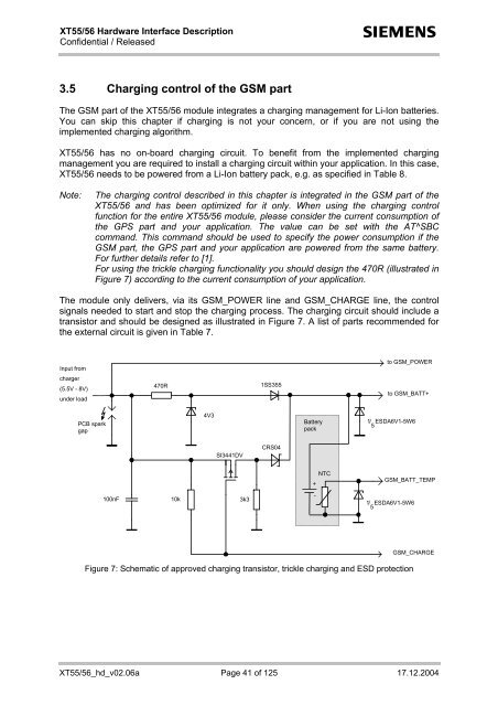
3.5 Charging control of the GSM part<br />
The GSM part of the XT55/56 module integrates a charging management for Li-Ion batteries.<br />
You can skip this chapter if charging is not your concern, or if you are not using the<br />
implemented charging algorithm.<br />
XT55/56 has no on-board charging circuit. To benefit from the implemented charging<br />
management you are required to install a charging circuit within your application. In this case,<br />
XT55/56 needs to be powered from a Li-Ion battery pack, e.g. as specified in Table 8.<br />
Note:<br />
The charging control described in this chapter is integrated in the GSM part of the<br />
XT55/56 and has been optimized for it only. When using the charging control<br />
function for the entire XT55/56 module, please consider the current consumption of<br />
the GPS part and your application. The value can be set with the AT^SBC<br />
command. This command should be used to specify the power consumption if the<br />
GSM part, the GPS part and your application are powered from the same battery.<br />
For further details refer to [1].<br />
For using the trickle charging functionality you should design the 470R (illustrated in<br />
Figure 7) according to the current consumption of your application.<br />
The module only delivers, via its GSM_POWER line and GSM_CHARGE line, the control<br />
signals needed to start and stop the charging process. The charging circuit should include a<br />
transistor and should be designed as illustrated in Figure 7. A list of parts recommended for<br />
the external circuit is given in Table 7.<br />
Input from<br />
to GSM_POWER<br />
charger<br />
(5.5V - 8V)<br />
under load<br />
470R<br />
1SS355<br />
to GSM_BATT+<br />
PCB spark<br />
gap<br />
4V3<br />
Battery<br />
pack<br />
1/ 5<br />
ESDA6V1-5W6<br />
SI3441DV<br />
CRS04<br />
+<br />
NTC<br />
GSM_BATT_TEMP<br />
100nF<br />
10k<br />
3k3<br />
-<br />
1/ 5<br />
ESDA6V1-5W6<br />
GSM_CHARGE<br />
Figure 7: Schematic of approved charging transistor, trickle charging and ESD protection<br />
XT55/56_hd_v02.06a Page 41 of 125 17.12.2004