Hardware Interface Description - KORE Telematics
Hardware Interface Description - KORE Telematics
Hardware Interface Description - KORE Telematics

You also want an ePaper? Increase the reach of your titles
YUMPU automatically turns print PDFs into web optimized ePapers that Google loves.
XT55/56 <strong>Hardware</strong> <strong>Interface</strong> <strong>Description</strong><br />
Confidential / Released<br />
s<br />
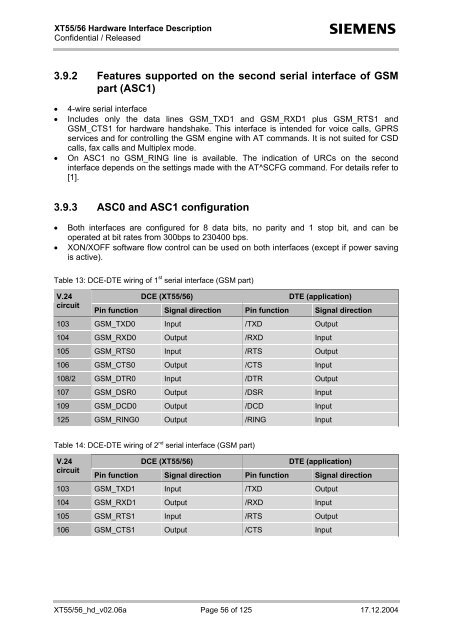
3.9.2 Features supported on the second serial interface of GSM<br />
part (ASC1)<br />
• 4-wire serial interface<br />
• Includes only the data lines GSM_TXD1 and GSM_RXD1 plus GSM_RTS1 and<br />
GSM_CTS1 for hardware handshake. This interface is intended for voice calls, GPRS<br />
services and for controlling the GSM engine with AT commands. It is not suited for CSD<br />
calls, fax calls and Multiplex mode.<br />
• On ASC1 no GSM_RING line is available. The indication of URCs on the second<br />
interface depends on the settings made with the AT^SCFG command. For details refer to<br />
[1].<br />
3.9.3 ASC0 and ASC1 configuration<br />
• Both interfaces are configured for 8 data bits, no parity and 1 stop bit, and can be<br />
operated at bit rates from 300bps to 230400 bps.<br />
• XON/XOFF software flow control can be used on both interfaces (except if power saving<br />
is active).<br />
Table 13: DCE-DTE wiring of 1 st serial interface (GSM part)<br />
V.24<br />
circuit<br />
DCE (XT55/56)<br />
DTE (application)<br />
Pin function Signal direction Pin function Signal direction<br />
103 GSM_TXD0 Input /TXD Output<br />
104 GSM_RXD0 Output /RXD Input<br />
105 GSM_RTS0 Input /RTS Output<br />
106 GSM_CTS0 Output /CTS Input<br />
108/2 GSM_DTR0 Input /DTR Output<br />
107 GSM_DSR0 Output /DSR Input<br />
109 GSM_DCD0 Output /DCD Input<br />
125 GSM_RING0 Output /RING Input<br />
Table 14: DCE-DTE wiring of 2 nd serial interface (GSM part)<br />
V.24<br />
circuit<br />
DCE (XT55/56)<br />
DTE (application)<br />
Pin function Signal direction Pin function Signal direction<br />
103 GSM_TXD1 Input /TXD Output<br />
104 GSM_RXD1 Output /RXD Input<br />
105 GSM_RTS1 Input /RTS Output<br />
106 GSM_CTS1 Output /CTS Input<br />
XT55/56_hd_v02.06a Page 56 of 125 17.12.2004