Functional overviewSTM<strong>32</strong>L162VD, STM<strong>32</strong>L162ZD, STM<strong>32</strong>L162QD, STM<strong>32</strong>L162RDNote:●●●Stop mode <strong>with</strong>out RTCStop mode achieves the lowest <strong>power</strong> consumption while retaining the RAM andregister contents. All clocks are stopped, the PLL, MSI RC, HSI and LSI RC, LSE andHSE crystal oscillators are disabled. The voltage regulator is in the low <strong>power</strong> mode.The device can be woken up from Stop mode by any of the EXTI line, in 8 µs. The EXTIline source can be one of the 16 external lines. It can be the PVD output, theComparator 1 event or Comparator 2 event (if internal reference voltage is on). It canalso be wakened by the USB wakeup.Standby mode <strong>with</strong> RTCStandby mode is used to achieve the lowest <strong>power</strong> consumption and real time clock.The internal voltage regulator is switched off so that the entire V CORE domain is<strong>power</strong>ed off. The PLL, MSI RC, HSI RC and HSE crystal oscillators are also switchedoff. The LSE or LSI is still running. After entering Standby mode, the RAM and registercontents are lost except for registers in the Standby circuitry (wakeup logic, IWDG,RTC, LSI, LSE Crystal <strong>32</strong>K osc, RCC_CSR).The device exits Standby mode in 60 µs when an external reset (NRST pin), an IWDGreset, a rising edge on one of the three WKUP pins, RTC alarm (Alarm A or Alarm B),RTC tamper event, RTC timestamp event or RTC Wakeup event occurs.Standby mode <strong>with</strong>out RTCStandby mode is used to achieve the lowest <strong>power</strong> consumption. The internal voltageregulator is switched off so that the entire V CORE domain is <strong>power</strong>ed off. The PLL, MSIRC, HSI and LSI RC, HSE and LSE crystal oscillators are also switched off. Afterentering Standby mode, the RAM and register contents are lost except for registers inthe Standby circuitry (wakeup logic, IWDG, RTC, LSI, LSE Crystal <strong>32</strong>K osc,RCC_CSR).The device exits Standby mode in 60 µs when an external reset (NRST pin) or a risingedge on one of the three WKUP pin occurs.The RTC, the IWDG, and the corresponding clock sources are not stopped automatically byentering Stop or Standby mode.3.2 <strong>ARM</strong> ® Cortex-M3 core <strong>with</strong> MPUThe <strong>ARM</strong> Cortex-M3 processor is the industry leading processor for embedded systems.It has been developed to provide a low-cost platform that meets the needs of <strong>MCU</strong>implementation, <strong>with</strong> a reduced pin count and low-<strong>power</strong> consumption, while deliveringoutstanding computational performance and an advanced system response to interrupts.The <strong>ARM</strong> Cortex-M3 <strong>32</strong>-<strong>bit</strong> RISC processor features exceptional code-efficiency,delivering the high-performance expected from an <strong>ARM</strong> core in the memory size usuallyassociated <strong>with</strong> 8- and 16-<strong>bit</strong> devices.The memory protection unit (MPU) improves system reliability by defining the memoryattributes (such as read/write access permissions) for different memory regions. It providesup to eight different regions and an optional predefined background region.Owing to its embedded <strong>ARM</strong> core, the STM<strong>32</strong>L162xD is compatible <strong>with</strong> all <strong>ARM</strong> tools andsoftware.14/124 Doc ID 022268 Rev 2
STM<strong>32</strong>L162VD, STM<strong>32</strong>L162ZD, STM<strong>32</strong>L162QD, STM<strong>32</strong>L162RDFunctional overviewNested vectored interrupt controller (NVIC)The ultralow <strong>power</strong> STM<strong>32</strong>L162xD embeds a nested vectored interrupt controller able tohandle up to 56 maskable interrupt channels (not including the 16 interrupt lines ofCortex-M3) and 16 priority levels.● Closely coupled NVIC gives low-latency interrupt processing● Interrupt entry vector table address passed directly to the core● Closely coupled NVIC core interface● Allows early processing of interrupts● Processing of late arriving, higher-priority interrupts●●●Support for tail-chainingProcessor state automatically savedInterrupt entry restored on interrupt exit <strong>with</strong> no instruction overheadThis hardware block provides flexible interrupt management features <strong>with</strong> minimal interruptlatency.3.3 Reset and supply management3.3.1 Power supply schemes●●V DD = 1.65 to 3.6 V: external <strong>power</strong> supply for I/Os and the internal regulator. Providedexternally through V DD pins.V SSA , V DDA = 1.65 to 3.6 V: external analog <strong>power</strong> supplies for ADC, reset blocks, RCsand PLL (minimum voltage to be applied to V DDA is 1.8 V when the ADC is used). V DDAand V SSA must be connected to V DD and V SS , respectively.3.3.2 Power supply supervisorThe device has an integrated ZEROPOWER <strong>power</strong>-on reset (POR)/<strong>power</strong>-down reset(PDR) that can be coupled <strong>with</strong> a brownout reset (BOR) circuitry.The device exists in two versions:● The version <strong>with</strong> BOR activated at <strong>power</strong>-on operates between 1.8 V and 3.6 V.● The other version <strong>with</strong>out BOR at <strong>power</strong> up operates between 1.65 V and 3.6 V.As the BOR can be activated and deactivated at run time, this distinction is important onlyfor <strong>power</strong>-up phase.When BOR is active at <strong>power</strong>-on, it ensures proper operation starting from 1.8 V whateverthe <strong>power</strong> ramp-up phase before it reaches 1.8 V. When BOR is not active at <strong>power</strong>-up, the<strong>power</strong> ramp-up should guarantee that 1.65 V is reached on V DD at least 1 ms after it exitsthe POR area.After the V DD threshold is reached (1.65 V or 1.8 V depending on the BOR which is active ornot at <strong>power</strong>-on), the option byte loading process starts, either to confirm or modify defaultthresholds, or to disable BOR permanently: in this case, the V DD min value at <strong>power</strong> down is1.65 V.Doc ID 022268 Rev 2 15/124
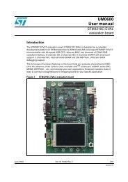
- Page 1 and 2: STM32L162VD STM32L162ZDSTM32L162QD
- Page 3 and 4: STM32L162VD, STM32L162ZD, STM32L162
- Page 6: List of tablesSTM32L162VD, STM32L16
- Page 9 and 10: STM32L162VD, STM32L162ZD, STM32L162
- Page 11 and 12: STM32L162VD, STM32L162ZD, STM32L162
- Page 13: STM32L162VD, STM32L162ZD, STM32L162
- Page 17 and 18: STM32L162VD, STM32L162ZD, STM32L162
- Page 19 and 20: STM32L162VD, STM32L162ZD, STM32L162
- Page 21 and 22: STM32L162VD, STM32L162ZD, STM32L162
- Page 24 and 25: Functional overviewSTM32L162VD, STM
- Page 26 and 27: Functional overviewSTM32L162VD, STM
- Page 28 and 29: Pin descriptionsSTM32L162VD, STM32L
- Page 30 and 31: Pin descriptionsSTM32L162VD, STM32L
- Page 32 and 33: Pin descriptionsSTM32L162VD, STM32L
- Page 34 and 35: Pin descriptionsSTM32L162VD, STM32L
- Page 36 and 37: Pin descriptionsSTM32L162VD, STM32L
- Page 38 and 39: 38/124 Doc ID 022268 Rev 2Table 6.P
- Page 40 and 41: 40/124 Doc ID 022268 Rev 2Table 6.P
- Page 42 and 43: 42/124 Doc ID 022268 Rev 2Table 6.P
- Page 44 and 45: 44/124 Doc ID 022268 Rev 2Table 6.P
- Page 46 and 47: 46/124 Doc ID 022268 Rev 2Table 6.P
- Page 48 and 49: Electrical characteristicsSTM32L162
- Page 50 and 51: Electrical characteristicsSTM32L162
- Page 52 and 53: Electrical characteristicsSTM32L162
- Page 54 and 55: Electrical characteristicsSTM32L162
- Page 56 and 57: Electrical characteristicsSTM32L162
- Page 58 and 59: Electrical characteristicsSTM32L162
- Page 60 and 61: Electrical characteristicsSTM32L162
- Page 62 and 63: Electrical characteristicsSTM32L162
- Page 64 and 65:
Electrical characteristicsSTM32L162
- Page 66 and 67:
Electrical characteristicsSTM32L162
- Page 68 and 69:
Electrical characteristicsSTM32L162
- Page 70 and 71:
Electrical characteristicsSTM32L162
- Page 72 and 73:
Electrical characteristicsSTM32L162
- Page 74 and 75:
Electrical characteristicsSTM32L162
- Page 76 and 77:
Electrical characteristicsSTM32L162
- Page 78 and 79:
Electrical characteristicsSTM32L162
- Page 80 and 81:
Electrical characteristicsSTM32L162
- Page 82 and 83:
Electrical characteristicsSTM32L162
- Page 84 and 85:
Electrical characteristicsSTM32L162
- Page 86 and 87:
Electrical characteristicsSTM32L162
- Page 88 and 89:
Electrical characteristicsSTM32L162
- Page 90 and 91:
Electrical characteristicsSTM32L162
- Page 92 and 93:
Electrical characteristicsSTM32L162
- Page 94 and 95:
Electrical characteristicsSTM32L162
- Page 96 and 97:
Electrical characteristicsSTM32L162
- Page 98 and 99:
Electrical characteristicsSTM32L162
- Page 100 and 101:
Electrical characteristicsSTM32L162
- Page 102 and 103:
Electrical characteristicsSTM32L162
- Page 104 and 105:
Electrical characteristicsSTM32L162
- Page 106 and 107:
Electrical characteristicsSTM32L162
- Page 108 and 109:
Electrical characteristicsSTM32L162
- Page 110 and 111:
Electrical characteristicsSTM32L162
- Page 112 and 113:
Electrical characteristicsSTM32L162
- Page 114 and 115:
Package characteristicsSTM32L162VD,
- Page 116 and 117:
Package characteristicsSTM32L162VD,
- Page 118 and 119:
Package characteristicsSTM32L162VD,
- Page 120 and 121:
Package characteristicsSTM32L162VD,
- Page 122 and 123:
Ordering information schemeSTM32L16
- Page 124:
STM32L162VD, STM32L162ZD, STM32L162