Physical Principles of Electron Microscopy: An Introduction to TEM ...
Physical Principles of Electron Microscopy: An Introduction to TEM ...
Physical Principles of Electron Microscopy: An Introduction to TEM ...

Create successful ePaper yourself
Turn your PDF publications into a flip-book with our unique Google optimized e-Paper software.
114 Chapter 4<br />
Crystals can also contain point defects, the simplest example being an<br />
a<strong>to</strong>mic vacancy: a missing a<strong>to</strong>m. Lattice planes become dis<strong>to</strong>rted in the<br />
immediate vicinity <strong>of</strong> the vacancy (as a<strong>to</strong>ms are pulled <strong>to</strong>wards the center)<br />
but only <strong>to</strong> a small degree, therefore single vacancies are not usually visible<br />
in a <strong>TEM</strong> image. However, the local strain produced by a cluster <strong>of</strong><br />
vacancies (a small void) gives rise <strong>to</strong> a characteristic bright/dark diffraction<br />
contrast; see Fig. 4-16.<br />
One example <strong>of</strong> a planar defect is the stacking fault, a plane within the<br />
crystal structure where the a<strong>to</strong>mic planes are abruptly displaced by a fraction<br />
<strong>of</strong> the intera<strong>to</strong>mic spacing. In a <strong>TEM</strong> image, the stacking fault gives rise <strong>to</strong> a<br />
series <strong>of</strong> narrowly-spaced fringes (see Fig. 4-15) whose explanation requires<br />
a Bloch-wave treatment <strong>of</strong> the electrons, as outlined below.<br />
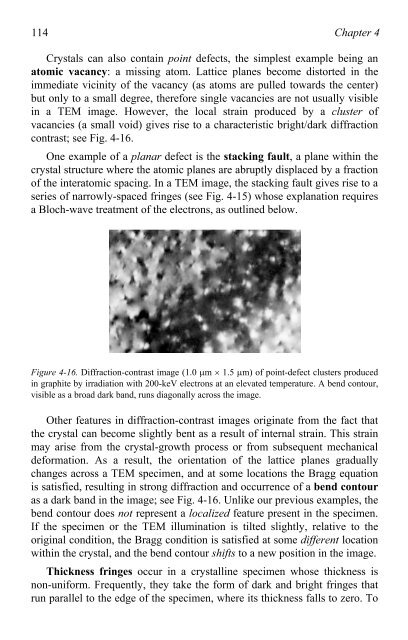
Figure 4-16. Diffraction-contrast image (1.0 �m � 1.5 �m) <strong>of</strong> point-defect clusters produced<br />
in graphite by irradiation with 200-keV electrons at an elevated temperature. A bend con<strong>to</strong>ur,<br />
visible as a broad dark band, runs diagonally across the image.<br />
Other features in diffraction-contrast images originate from the fact that<br />
the crystal can become slightly bent as a result <strong>of</strong> internal strain. This strain<br />
may arise from the crystal-growth process or from subsequent mechanical<br />
deformation. As a result, the orientation <strong>of</strong> the lattice planes gradually<br />
changes across a <strong>TEM</strong> specimen, and at some locations the Bragg equation<br />
is satisfied, resulting in strong diffraction and occurrence <strong>of</strong> a bend con<strong>to</strong>ur<br />
as a dark band in the image; see Fig. 4-16. Unlike our previous examples, the<br />
bend con<strong>to</strong>ur does not represent a localized feature present in the specimen.<br />
If the specimen or the <strong>TEM</strong> illumination is tilted slightly, relative <strong>to</strong> the<br />
original condition, the Bragg condition is satisfied at some different location<br />
within the crystal, and the bend con<strong>to</strong>ur shifts <strong>to</strong> a new position in the image.<br />
Thickness fringes occur in a crystalline specimen whose thickness is<br />
non-uniform. Frequently, they take the form <strong>of</strong> dark and bright fringes that<br />
run parallel <strong>to</strong> the edge <strong>of</strong> the specimen, where its thickness falls <strong>to</strong> zero. To