Physical Principles of Electron Microscopy: An Introduction to TEM ...
Physical Principles of Electron Microscopy: An Introduction to TEM ...
Physical Principles of Electron Microscopy: An Introduction to TEM ...

Create successful ePaper yourself
Turn your PDF publications into a flip-book with our unique Google optimized e-Paper software.
Recent Developments 179<br />
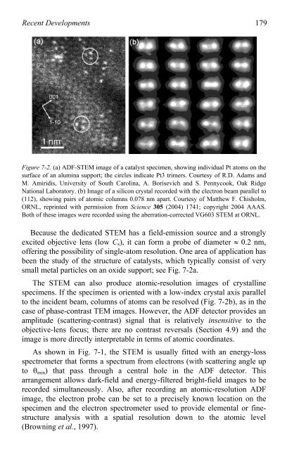
Figure 7-2. (a) ADF-S<strong>TEM</strong> image <strong>of</strong> a catalyst specimen, showing individual Pt a<strong>to</strong>ms on the<br />
surface <strong>of</strong> an alumina support; the circles indicate Pt3 trimers. Courtesy <strong>of</strong> R.D. Adams and<br />
M. Amiridis, University <strong>of</strong> South Carolina, A. Borisevich and S. Pennycook, Oak Ridge<br />
National Labora<strong>to</strong>ry. (b) Image <strong>of</strong> a silicon crystal recorded with the electron beam parallel <strong>to</strong><br />
(112), showing pairs <strong>of</strong> a<strong>to</strong>mic columns 0.078 nm apart. Courtesy <strong>of</strong> Matthew F. Chisholm,<br />
ORNL, reprinted with permission from Science 305 (2004) 1741; copyright 2004 AAAS.<br />
Both <strong>of</strong> these images were recorded using the aberration-corrected VG603 S<strong>TEM</strong> at ORNL.<br />
Because the dedicated S<strong>TEM</strong> has a field-emission source and a strongly<br />
excited objective lens (low Cs), it can form a probe <strong>of</strong> diameter � 0.2 nm,<br />
<strong>of</strong>fering the possibility <strong>of</strong> single-a<strong>to</strong>m resolution. One area <strong>of</strong> application has<br />
been the study <strong>of</strong> the structure <strong>of</strong> catalysts, which typically consist <strong>of</strong> very<br />
small<br />
metal particles on an oxide support; see Fig. 7-2a.<br />
The S<strong>TEM</strong> can also produce a<strong>to</strong>mic-resolution images <strong>of</strong> crystalline<br />
specimens. If the specimen is oriented with a low-index crystal axis parallel<br />
<strong>to</strong> the incident beam, columns <strong>of</strong> a<strong>to</strong>ms can be resolved (Fig. 7-2b), as in the<br />
case <strong>of</strong> phase-contrast <strong>TEM</strong> images. However, the ADF detec<strong>to</strong>r provides an<br />
amplitude (scattering-contrast) signal that is relatively insensitive <strong>to</strong> the<br />
objective-lens focus; there are no contrast reversals (Section 4.9) and the<br />
image<br />
is more directly interpretable in terms <strong>of</strong> a<strong>to</strong>mic coordinates.<br />
As shown in Fig. 7-1, the S<strong>TEM</strong> is usually fitted with an energy-loss<br />
spectrometer that forms a spectrum from electrons (with scattering angle up<br />
<strong>to</strong> �min) that pass through a central hole in the ADF detec<strong>to</strong>r. This<br />
arrangement allows dark-field and energy-filtered bright-field images <strong>to</strong> be<br />
recorded simultaneously. Also, after recording an a<strong>to</strong>mic-resolution ADF<br />
image, the electron probe can be set <strong>to</strong> a precisely known location on the<br />
specimen and the electron spectrometer used <strong>to</strong> provide elemental or finestructure<br />
analysis with a spatial resolution down <strong>to</strong> the a<strong>to</strong>mic level<br />
(Browning et al., 1997).