Physical Principles of Electron Microscopy: An Introduction to TEM ...
Physical Principles of Electron Microscopy: An Introduction to TEM ...
Physical Principles of Electron Microscopy: An Introduction to TEM ...

You also want an ePaper? Increase the reach of your titles
YUMPU automatically turns print PDFs into web optimized ePapers that Google loves.
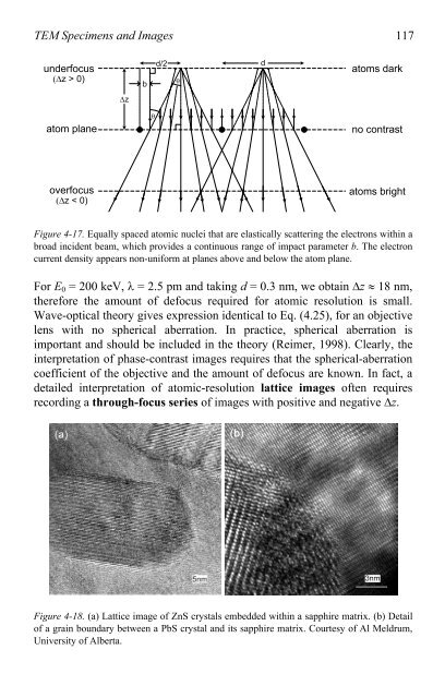
<strong>TEM</strong> Specimens and Images 117<br />
underfocus a<strong>to</strong>ms dark<br />
��z > 0) �<br />
a<strong>to</strong>m plane<br />
�z<br />
b<br />
�<br />
d/2<br />
no contrast<br />
overfocus a<strong>to</strong>ms bright<br />
��z < 0)<br />
Figure 4-17. Equally spaced a<strong>to</strong>mic nuclei that are elastically scattering the electrons within a<br />
broad incident beam, which provides a continuous range <strong>of</strong> impact parameter b. The electron<br />
current density appears non-uniform at planes above and below the a<strong>to</strong>m plane.<br />
For E0 = 200 keV, � = 2.5 pm and taking d = 0.3 nm, we obtain �z � 18 nm,<br />
therefore the amount <strong>of</strong> defocus required for a<strong>to</strong>mic resolution is small.<br />
Wave-optical theory gives expression identical <strong>to</strong> Eq. (4.25), for an objective<br />
lens with no spherical aberration. In practice, spherical aberration is<br />
important and should be included in the theory (Reimer, 1998). Clearly, the<br />
interpretation <strong>of</strong> phase-contrast images requires that the spherical-aberration<br />
coefficient <strong>of</strong> the objective and the amount <strong>of</strong> defocus are known. In fact, a<br />
detailed interpretation <strong>of</strong> a<strong>to</strong>mic-resolution lattice images <strong>of</strong>ten requires<br />
recording a through-focus series <strong>of</strong> images with positive and negative �z.<br />
Figure 4-18. (a) Lattice image <strong>of</strong> ZnS crystals embedded within a sapphire matrix. (b) Detail<br />
<strong>of</strong> a grain boundary between a PbS crystal and its sapphire matrix. Courtesy <strong>of</strong> Al Meldrum,<br />
University <strong>of</strong> Alberta.<br />
d