

DS1036 - Platform Manager Data Sheet - Lattice Semiconductor
DS1036 - Platform Manager Data Sheet - Lattice Semiconductor
DS1036 - Platform Manager Data Sheet - Lattice Semiconductor

You also want an ePaper? Increase the reach of your titles
YUMPU automatically turns print PDFs into web optimized ePapers that Google loves.
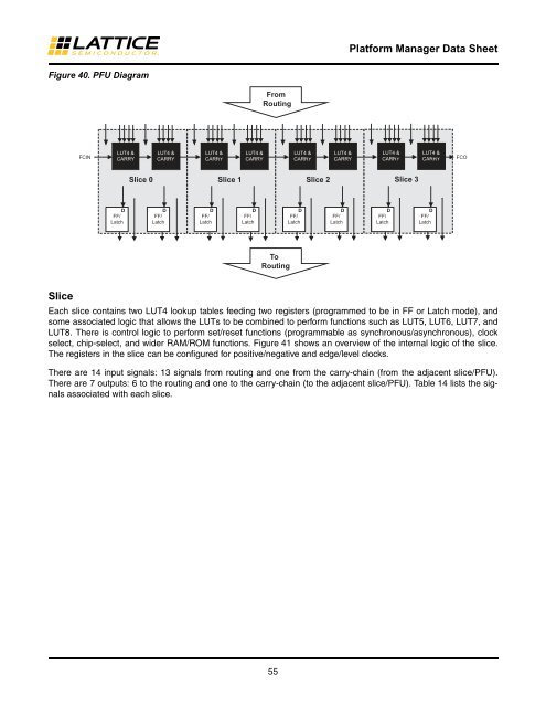
Figure 40. PFU Diagram<br />
Slice<br />
Slice 0<br />
55<br />
<strong>Platform</strong> <strong>Manager</strong> <strong>Data</strong> <strong>Sheet</strong><br />
LUT4 & LUT4 &<br />
LUT4 & LUT4 &<br />
LUT4 & LUT4 &<br />
LUT4 & LUT4 &<br />
FCIN CARRY CARRY<br />
CARRY CARRY<br />
CARRY CARRY<br />
CARRY CARRY FCO<br />
D<br />
FF/<br />
Latch<br />
D<br />
FF/<br />
Latch<br />
D<br />
FF/<br />
Latch<br />
Slice 1<br />
D<br />
FF/<br />
Latch<br />
From<br />
Routin g<br />
To<br />
Routin g<br />
Slice 2<br />
Slice 3<br />
Each slice contains two LUT4 lookup tables feeding two registers (programmed to be in FF or Latch mode), and<br />
some associated logic that allows the LUTs to be combined to perform functions such as LUT5, LUT6, LUT7, and<br />
LUT8. There is control logic to perform set/reset functions (programmable as synchronous/asynchronous), clock<br />
select, chip-select, and wider RAM/ROM functions. Figure 41 shows an overview of the internal logic of the slice.<br />
The registers in the slice can be configured for positive/negative and edge/level clocks.<br />
There are 14 input signals: 13 signals from routing and one from the carry-chain (from the adjacent slice/PFU).<br />
There are 7 outputs: 6 to the routing and one to the carry-chain (to the adjacent slice/PFU). Table 14 lists the signals<br />
associated with each slice.<br />
D<br />
FF/<br />
Latch<br />
D<br />
FF/<br />
Latch<br />
D<br />
FF/<br />
Latch<br />
D<br />
FF/<br />
Latch


