

DS1036 - Platform Manager Data Sheet - Lattice Semiconductor
DS1036 - Platform Manager Data Sheet - Lattice Semiconductor
DS1036 - Platform Manager Data Sheet - Lattice Semiconductor

You also want an ePaper? Increase the reach of your titles
YUMPU automatically turns print PDFs into web optimized ePapers that Google loves.
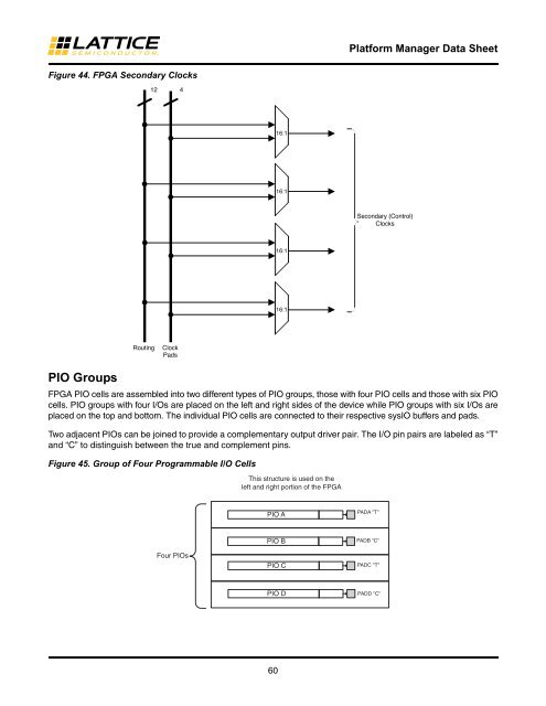
Figure 44. FPGA Secondary Clocks<br />
PIO Groups<br />
12<br />
Routing Clock<br />
Pads<br />
60<br />
<strong>Platform</strong> <strong>Manager</strong> <strong>Data</strong> <strong>Sheet</strong><br />
FPGA PIO cells are assembled into two different types of PIO groups, those with four PIO cells and those with six PIO<br />
cells. PIO groups with four I/Os are placed on the left and right sides of the device while PIO groups with six I/Os are<br />
placed on the top and bottom. The individual PIO cells are connected to their respective sysIO buffers and pads.<br />
Two adjacent PIOs can be joined to provide a complementary output driver pair. The I/O pin pairs are labeled as “T”<br />
and “C” to distinguish between the true and complement pins.<br />
Figure 45. Group of Four Programmable I/O Cells<br />
4<br />
Four PIOs<br />
16:1<br />
16:1<br />
16:1<br />
16:1<br />
This structure is used on the<br />
left and right portion of the FPGA<br />
PIO A<br />
PIO B<br />
PIO C<br />
PIO D<br />
Secondary (Control)<br />
Clocks<br />
PADA "T"<br />
PADB "C"<br />
PADC "T"<br />
PADD "C"


