

DS1036 - Platform Manager Data Sheet - Lattice Semiconductor
DS1036 - Platform Manager Data Sheet - Lattice Semiconductor
DS1036 - Platform Manager Data Sheet - Lattice Semiconductor

Create successful ePaper yourself
Turn your PDF publications into a flip-book with our unique Google optimized e-Paper software.
63<br />
<strong>Platform</strong> <strong>Manager</strong> <strong>Data</strong> <strong>Sheet</strong><br />
banks that are critical to the application. The default configuration of the I/O pins in a blank device is tri-state with a<br />
weak pull-up to V CCIO . The I/O pins will maintain the blank configuration until V CC , V CCAUX and V CCIO have<br />
reached satisfactory levels at which time the I/Os will take on the user-configured settings.<br />
The V CC and V CCAUX supply the power to the FPGA core fabric, whereas the V CCIO supplies power to the I/O buffers.<br />
In order to simplify system design while providing consistent and predictable I/O behavior, the I/O buffers<br />
should be powered up along with the FPGA core fabric. Therefore, V CCIO supplies should be powered up together<br />
with the V CC and V CCAUX supplies. (V CC and V CCAUX must be physically tied together for proper operation).<br />
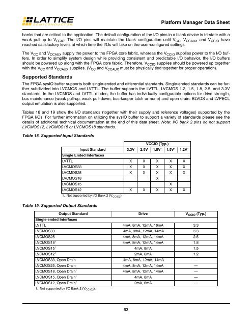
Supported Standards<br />
The FPGA sysIO buffer supports both single-ended and differential standards. Single-ended standards can be further<br />
subdivided into LVCMOS and LVTTL. The buffer supports the LVTTL, LVCMOS 1.2, 1.5, 1.8, 2.5, and 3.3V<br />
standards. In the LVCMOS and LVTTL modes, the buffer has individually configurable options for drive strength,<br />
bus maintenance (weak pull-up, weak pull-down, bus-keeper latch or none) and open drain. BLVDS and LVPECL<br />
output emulation is also supported.<br />
Tables 18 and 19 show the I/O standards (together with their supply and reference voltages) supported by the<br />
FPGA I/Os. For further information on utilizing the sysIO buffer to support a variety of standards please see the<br />
details of additional technical documentation at the end of this data sheet. Note: I/O bank 2 pins do not support<br />
LVCMOS12, LVCMOS15 or LVCMOS18 standards.<br />
Table 18. Supported Input Standards<br />
Table 19. Supported Output Standards<br />
VCCIO (Typ.)<br />
Input Standard 3.3V 2.5V 1.8V 1<br />
1.5V 1<br />
Single Ended Interfaces<br />
LVTTL X X X X X<br />
LVCMOS33 X X X X X<br />
LVCMOS25 X X X X X<br />
LVCMOS18 X<br />
LVCMOS15 X<br />
LVCMOS12<br />
1. Not supported by I/O Bank 2 (VCCIO2 ).<br />
X X X X X<br />
1.2V 1<br />
Output Standard<br />
Single-ended Interfaces<br />
Drive VCCIO (Typ.)<br />
LVTTL 4mA, 8mA, 12mA, 16mA 3.3<br />
LVCMOS33 4mA, 8mA, 12mA, 14mA 3.3<br />
LVCMOS25 4mA, 8mA, 12mA, 14mA 2.5<br />
LVCMOS18 1<br />
4mA, 8mA, 12mA, 14mA 1.8<br />
LVCMOS15 1<br />
4mA, 8mA 1.5<br />
LVCMOS12 1<br />
2mA, 6mA 1.2<br />
LVCMOS33, Open Drain 4mA, 8mA, 12mA, 14mA —<br />
LVCMOS25, Open Drain 4mA, 8mA, 12mA, 14mA —<br />
LVCMOS18, Open Drain1 4mA, 8mA, 12mA, 14mA —<br />
LVCMOS15, Open Drain 1<br />
4mA, 8mA —<br />
LVCMOS12, Open Drain1 1. Not supported by I/O Bank 2 (VCCIO2). 2mA, 6mA —


