

DS1036 - Platform Manager Data Sheet - Lattice Semiconductor
DS1036 - Platform Manager Data Sheet - Lattice Semiconductor
DS1036 - Platform Manager Data Sheet - Lattice Semiconductor

You also want an ePaper? Increase the reach of your titles
YUMPU automatically turns print PDFs into web optimized ePapers that Google loves.
1, 2, 3, 4<br />
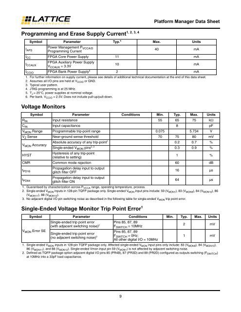
Programming and Erase Supply Current<br />
Voltage Monitors<br />
Single-Ended Voltage Monitor Trip Point Error 1<br />
9<br />
<strong>Platform</strong> <strong>Manager</strong> <strong>Data</strong> <strong>Sheet</strong><br />
Symbol Parameter Typ. 5<br />
Max. Units<br />
IAPS Power Management PVCCA/D Programming Current<br />
40 mA<br />
ICC FPGA Core Power Supply 11 mA<br />
ICCAUX FPGA Auxiliary Power Supply<br />
VCCAUX = 3.3V<br />
10 mA<br />
ICCIO FPGA Bank Power Supply 6<br />
2 mA<br />
1. For further information on supply current, please see details of additional technical documentation at the end of this data sheet.<br />
2. Assumes all I/O pins are held at VCCIO or GND.<br />
3. Typical user pattern.<br />
4. JTAG programming is at 25 MHz.<br />
5. TJ = 25°C, power supplies at nominal voltage.<br />
6. Per bank. VCCIO = 2.5V. Does not include pull-up/pull-down.<br />
Symbol Parameter Conditions Min. Typ. Max. Units<br />
RIN Input resistance 55 65 75 k�<br />
CIN Input capacitance 8 pF<br />
VMON Range Programmable trip-point range 0.075 5.734 V<br />
VZ Sense Near-ground sense threshold 70 75 80 mV<br />
V MON Accuracy<br />
Absolute accuracy of any trip-point 1<br />
2, 3<br />
Single-ended VMON pins<br />
0.2 0.7 %<br />
0.3 0.9 %<br />
HYST<br />
Hysteresis of any trip-point<br />
(relative to setting)<br />
1 %<br />
CMR Common mode rejection 60 dB<br />
tPD16 Propagation delay input to output<br />
glitch filter OFF<br />
16 µs<br />
tPD64 Propagation delay input to output<br />
glitch filter ON<br />
64 µs<br />
1. Guaranteed by characterization across P VCCA range, operating temperature, process.<br />
2. Single-ended V MON inputs in 128-pin TQFP package only. Single-ended V MON input pins include: 59 (V MON1 ), 83 (V MON9 ), 84 (V MON10 ), 86<br />
(V MON11), 88 (V MON12).<br />
3. No adjacent digital I/O pin switching noise as described in the following table for single-ended V MON trip point error.<br />
Symbol Parameter Conditions Min. Typ. Max. Units<br />
V MON Error SE<br />
Single-ended trip point error<br />
(with adjacent switching noise) 2<br />
Single-ended trip point error<br />
(no adjacent switching noise) 2<br />
Pins 85, 87, 89<br />
FSWITCH = 10MHz<br />
Pins 85, 87, 89<br />
FSWITCH = 0Hz;<br />
All other digital I/O = 10MHz<br />
2 mV<br />
1 mV<br />
1. Single-ended V MON inputs in 128-pin TQFP package only. Affected single-ended V MON input pins only include: 83 (V MON9), 84 (V MON10),<br />
86 (V MON11 ), and 88 (V MON12 ). Single-ended Vmon input pin 59 (V MON1 ) is not affected by adjacent switching noise.<br />
2. Defined as TQFP package option adjacent digital I/O pins 85 (PR4B), 87 (PR3D) and 89 (PR2D) configured as outputs switching (F SWITCH)<br />
at 10MHz into a 33pF load capacitance.


