

DS1036 - Platform Manager Data Sheet - Lattice Semiconductor
DS1036 - Platform Manager Data Sheet - Lattice Semiconductor
DS1036 - Platform Manager Data Sheet - Lattice Semiconductor

Create successful ePaper yourself
Turn your PDF publications into a flip-book with our unique Google optimized e-Paper software.
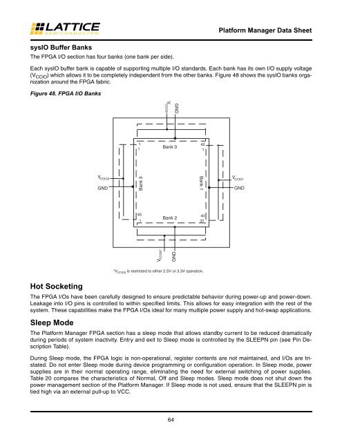
sysIO Buffer Banks<br />
The FPGA I/O section has four banks (one bank per side).<br />
64<br />
<strong>Platform</strong> <strong>Manager</strong> <strong>Data</strong> <strong>Sheet</strong><br />
Each sysIO buffer bank is capable of supporting multiple I/O standards. Each bank has its own I/O supply voltage<br />
(V CCIO ) which allows it to be completely independent from the other banks. Figure 48 shows the sysIO banks organization<br />
around the FPGA fabric.<br />
Figure 48. FPGA I/O Banks<br />
Hot Socketing<br />
The FPGA I/Os have been carefully designed to ensure predictable behavior during power-up and power-down.<br />
Leakage into I/O pins is controlled to within specified limits. This allows for easy integration with the rest of the<br />
system. These capabilities make the FPGA I/Os ideal for many multiple power supply and hot-swap applications.<br />
Sleep Mode<br />
V CCIO3<br />
1<br />
1<br />
GND Bank 3<br />
GND<br />
The <strong>Platform</strong> <strong>Manager</strong> FPGA section has a sleep mode that allows standby current to be reduced dramatically<br />
during periods of system inactivity. Entry and exit to Sleep mode is controlled by the SLEEPN pin (see Pin Description<br />
Table).<br />
During Sleep mode, the FPGA logic is non-operational, register contents are not maintained, and I/Os are tristated.<br />
Do not enter Sleep mode during device programming or configuration operation. In Sleep mode, power<br />
supplies are in their normal operating range, eliminating the need for external switching of power supplies.<br />
Table 20 compares the characteristics of Normal, Off and Sleep modes. Sleep mode does not shut down the<br />
power management section of the <strong>Platform</strong> <strong>Manager</strong>. If Sleep mode is not used, ensure that the SLEEPN pin is<br />
tied high via an external pull-up to VCC.<br />
Bank 1<br />
40<br />
40<br />
Bank 2<br />
1 37<br />
V CCIO2*<br />
*V CCIO2 is restricted to either 2.5V or 3.3V operation.<br />
V CCIO0<br />
Bank 0<br />
GND<br />
42<br />
1<br />
V CCIO1<br />
GND


