

Parallel Flash Loader Megafunction User Guide (PDF) - Altera
Parallel Flash Loader Megafunction User Guide (PDF) - Altera
Parallel Flash Loader Megafunction User Guide (PDF) - Altera

You also want an ePaper? Increase the reach of your titles
YUMPU automatically turns print PDFs into web optimized ePapers that Google loves.
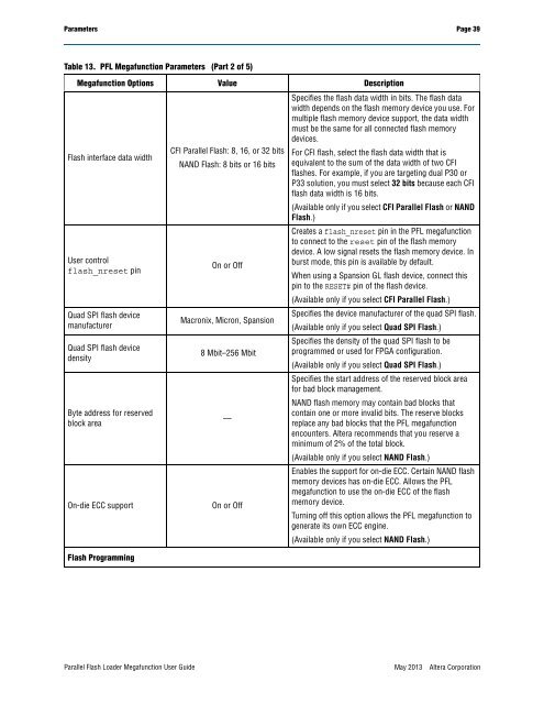
Parameters Page 39<br />
Table 13. PFL <strong>Megafunction</strong> Parameters (Part 2 of 5)<br />
<strong>Megafunction</strong> Options Value Description<br />
<strong>Flash</strong> interface data width<br />
<strong>User</strong> control<br />
flash_nreset pin<br />
Quad SPI flash device<br />
manufacturer<br />
Quad SPI flash device<br />
density<br />
Byte address for reserved<br />
block area<br />
On-die ECC support<br />
<strong>Flash</strong> Programming<br />
CFI <strong>Parallel</strong> <strong>Flash</strong>: 8, 16, or 32 bits<br />
NAND <strong>Flash</strong>: 8 bits or 16 bits<br />
On or Off<br />
Macronix, Micron, Spansion<br />
8 Mbit–256 Mbit<br />
—<br />
On or Off<br />
Specifies the flash data width in bits. The flash data<br />
width depends on the flash memory device you use. For<br />
multiple flash memory device support, the data width<br />
must be the same for all connected flash memory<br />
devices.<br />
For CFI flash, select the flash data width that is<br />
equivalent to the sum of the data width of two CFI<br />
flashes. For example, if you are targeting dual P30 or<br />
P33 solution, you must select 32 bits because each CFI<br />
flash data width is 16 bits.<br />
(Available only if you select CFI <strong>Parallel</strong> <strong>Flash</strong> or NAND<br />
<strong>Flash</strong>.)<br />
Creates a flash_nreset pin in the PFL megafunction<br />
to connect to the reset pin of the flash memory<br />
device. A low signal resets the flash memory device. In<br />
burst mode, this pin is available by default.<br />
When using a Spansion GL flash device, connect this<br />
pin to the RESET# pin of the flash device.<br />
(Available only if you select CFI <strong>Parallel</strong> <strong>Flash</strong>.)<br />
Specifies the device manufacturer of the quad SPI flash.<br />
(Available only if you select Quad SPI <strong>Flash</strong>.)<br />
Specifies the density of the quad SPI flash to be<br />
programmed or used for FPGA configuration.<br />
(Available only if you select Quad SPI <strong>Flash</strong>.)<br />
Specifies the start address of the reserved block area<br />
for bad block management.<br />
NAND flash memory may contain bad blocks that<br />
contain one or more invalid bits. The reserve blocks<br />
replace any bad blocks that the PFL megafunction<br />
encounters. <strong>Altera</strong> recommends that you reserve a<br />
minimum of 2% of the total block.<br />
(Available only if you select NAND <strong>Flash</strong>.)<br />
Enables the support for on-die ECC. Certain NAND flash<br />
memory devices has on-die ECC. Allows the PFL<br />
megafunction to use the on-die ECC of the flash<br />
memory device.<br />
Turning off this option allows the PFL megafunction to<br />
generate its own ECC engine.<br />
(Available only if you select NAND <strong>Flash</strong>.)<br />
<strong>Parallel</strong> <strong>Flash</strong> <strong>Loader</strong> <strong>Megafunction</strong> <strong>User</strong> <strong>Guide</strong><br />
May 2013<br />
<strong>Altera</strong> Corporation


