

Parallel Flash Loader Megafunction User Guide (PDF) - Altera
Parallel Flash Loader Megafunction User Guide (PDF) - Altera
Parallel Flash Loader Megafunction User Guide (PDF) - Altera

Create successful ePaper yourself
Turn your PDF publications into a flip-book with our unique Google optimized e-Paper software.
Page 46<br />
Specifications<br />
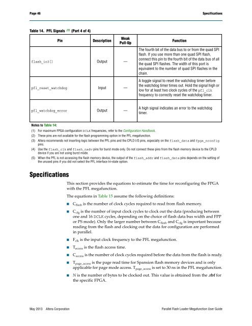
Table 14. PFL Signals (1) (Part 4 of 4)<br />
Pin<br />
Description<br />
Weak<br />
Pull-Up<br />
flash_io3[] Output —<br />
pfl_reset_watchdog Input —<br />
Function<br />
The fourth bit of the data bus to or from the quad SPI<br />
flash. If you use more than one quad SPI flash,<br />
connect this pin to the fourth bit of the data bus of all<br />
the quad SPI flashes. The width of this port is<br />
equivalent to the number of quad SPI flashes in the<br />
chain.<br />
A toggle signal to reset the watchdog timer before<br />
the watchdog timer times out. Hold the signal high or<br />
low for at least two clock cycles of the pfl_clk<br />
frequency to correctly reset the watchdog timer.<br />
pfl_watchdog_error Output —<br />
A high signal indicates an error to the watchdog<br />
timer.<br />
Notes to Table 14:<br />
(1) For maximum FPGA configuration DCLK frequencies, refer to the Configuration Handbook.<br />
(2) These pins are not available for the flash programming option in the PFL megafunction.<br />
(3) <strong>Altera</strong> recommends not inserting logic between the PFL pins and the CPLD I/O pins, especially on the flash_data and fpga_nconfig<br />
pins.<br />
(4) Use the flash_clk and flash_nadv pins for burst mode only. Do not connect these pins from the flash memory device to the CPLD<br />
device if you are not using burst mode.<br />
(5) When the PFL is not accessing the flash memory device, the output of the flash_addr and flash_data pins depends on the setting of<br />
the unused pins if you did not select the PFL interface tri-state option.<br />
Specifications<br />
This section provides the equations to estimate the time for reconfiguring the FPGA<br />
with the PFL megafunction.<br />
The equations in Table 15 assume the following definitions:<br />
■<br />
■<br />
■<br />
■<br />
■<br />
■<br />
■<br />
C flash is the number of clock cycles required to read from flash memory.<br />
C cfg is the number of input clock cycles to clock out the data (producing between<br />
one and 16 DCLK cycles, depending on the choice of flash data bus width and FPP<br />
or PS mode). Only the larger number between C flash and C cfg is important because<br />
reading from the flash and clocking out the data for configuration are performed<br />
in parallel.<br />
F clk is the input clock frequency to the PFL megafunction.<br />
T access is the flash access time.<br />
C access is the number of clock cycles required before the data from the flash is ready.<br />
T page_access is the page read time for Spansion flash memory devices and is only<br />
applicable for page mode access. T page_access is set to 30 ns in the PFL megafunction.<br />
N is the number of bytes to be clocked out. This value is obtained from the .rbf for<br />
the specific FPGA.<br />
May 2013 <strong>Altera</strong> Corporation <strong>Parallel</strong> <strong>Flash</strong> <strong>Loader</strong> <strong>Megafunction</strong> <strong>User</strong> <strong>Guide</strong>


