

Parallel Flash Loader Megafunction User Guide (PDF) - Altera
Parallel Flash Loader Megafunction User Guide (PDF) - Altera
Parallel Flash Loader Megafunction User Guide (PDF) - Altera

Create successful ePaper yourself
Turn your PDF publications into a flip-book with our unique Google optimized e-Paper software.
Page 40<br />
Parameters<br />
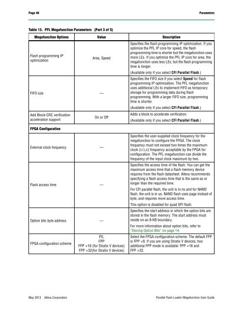
Table 13. PFL <strong>Megafunction</strong> Parameters (Part 3 of 5)<br />
<strong>Megafunction</strong> Options Value Description<br />
<strong>Flash</strong> programming IP<br />
optimization<br />
Area, Speed<br />
FIFO size —<br />
Add Block-CRC verification<br />
acceleration support<br />
FPGA Configuration<br />
On or Off<br />
Specifies the flash programming IP optimization. If you<br />
optimize the PFL IP core for speed, the flash<br />
programming time is shorter but the megafunction uses<br />
more LEs. If you optimize the PFL IP core for area, the<br />
megafunction uses less LEs, but the flash programming<br />
time is longer.<br />
(Available only if you select CFI <strong>Parallel</strong> <strong>Flash</strong>.)<br />
Specifies the FIFO size if you select Speed for flash<br />
programming IP optimization. The PFL megafunction<br />
uses additional LEs to implement FIFO as temporary<br />
storage for programming data during flash<br />
programming. With a larger FIFO size, programming<br />
time is shorter.<br />
(Available only if you select CFI <strong>Parallel</strong> <strong>Flash</strong>.)<br />
Adds a block to accelerate verification.<br />
(Available only if you select CFI <strong>Parallel</strong> <strong>Flash</strong>.)<br />
External clock frequency —<br />
<strong>Flash</strong> access time —<br />
Option bits byte address —<br />
FPGA configuration scheme<br />
PS,<br />
FPP<br />
FPP ×16 (for Stratix V devices)<br />
FPP ×32(for Stratix V devices)<br />
Specifies the user-supplied clock frequency for the<br />
megafunction to configure the FPGA. The clock<br />
frequency must not exceed two times the maximum<br />
clock (DCLK) frequency acceptable by the FPGA for<br />
configuration. The PFL megafunction can divide the<br />
frequency of the input clock maximum by two.<br />
Specifies the access time of the flash. You can get the<br />
maximum access time that a flash memory device<br />
requires from the flash datasheet. <strong>Altera</strong> recommends<br />
specifying a flash access time that is the same as or<br />
longer than the required time.<br />
For CFI parallel flash, the unit is in ns and for NAND<br />
flash, the unit is in us. NAND flash uses page instead of<br />
byte, and requires more access time.<br />
This option is disabled for quad SPI flash.<br />
Specifies the start address in which the option bits are<br />
stored in the flash memory. The start address must<br />
reside on an 8-KB boundary.<br />
For more information about option bits, refer to<br />
“Storing Option Bits” on page 14.<br />
Select the FPGA configuration scheme. The default FPP<br />
is FPP ×8. If you are using Stratix V devices, two<br />
additional FPP mode is available: FPP ×16 and<br />
FPP ×32.<br />
May 2013 <strong>Altera</strong> Corporation <strong>Parallel</strong> <strong>Flash</strong> <strong>Loader</strong> <strong>Megafunction</strong> <strong>User</strong> <strong>Guide</strong>


