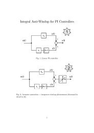
Direct Power and Torque Control of AC/DC/AC Converter-Fed ...
Direct Power and Torque Control of AC/DC/AC Converter-Fed ...
Direct Power and Torque Control of AC/DC/AC Converter-Fed ...

You also want an ePaper? Increase the reach of your titles
YUMPU automatically turns print PDFs into web optimized ePapers that Google loves.
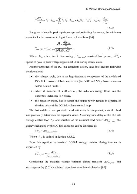
5. Passive Components Design<br />
dU<br />
C<br />
dt<br />
C<br />
dc<br />
= Idc<br />
− Iload<br />
= ∑ ILk<br />
k = A<br />
S<br />
k<br />
− I<br />
load<br />
≈ I<br />
LA<br />
S<br />
A<br />
+ I<br />
LB<br />
S<br />
B<br />
+ I<br />
LC<br />
S<br />
C<br />
P<br />
−<br />
U<br />
(5. 2)<br />
For given allowable peak ripple voltage <strong>and</strong> switching frequency, the minimum<br />
capacitor for the converter in Fig.4. 1 can be found from [24]:<br />
C<br />
min_VSR1<br />
3U<br />
LL<br />
2 +<br />
Udc<br />
= Pload<br />
_ max<br />
,<br />
(5. 3)<br />
2 3∆U<br />
f U<br />
dc<br />
s<br />
LL<br />
load<br />
dc<br />
Where:<br />
U<br />
LL<br />
- is a line to line voltage,<br />
load _ max<br />
P - maximal load power, ∆U<br />
dc<br />
-<br />
specified peak to peak voltage ripple in <strong>DC</strong>-link during steady states.<br />
Another approach <strong>of</strong> the <strong>DC</strong>-link capacitors design, takes into account following<br />
considerations:<br />
• the voltage ripple, due to the high-frequency components <strong>of</strong> the modulated<br />
<strong>DC</strong>- link currents <strong>of</strong> both converters (i.e. VSR <strong>and</strong> VSI), have to remain<br />
within desired limits,<br />
• when all switches <strong>of</strong> VSR are <strong>of</strong>f, the inductors energy flows into the<br />
capacitor, increasing its voltage,<br />
• the capacitor energy has to sustain the output power dem<strong>and</strong> in a period <strong>of</strong><br />
the time delay <strong>of</strong> the <strong>DC</strong>-link voltage control loop.<br />
The first <strong>and</strong> the second point <strong>of</strong> considerations are less important, while the third<br />
one practically determines the capacitor value. Assuming time delay <strong>of</strong> the <strong>DC</strong>-link<br />
voltage control loop T UT<br />
<strong>and</strong> variation <strong>of</strong> the maximal load power ∆ P load _ max , the<br />
energy exchanged by the <strong>DC</strong>-link capacitor can be estimated as:<br />
∆ W = ∆P T<br />
(5. 4)<br />
dc<br />
load _ max<br />
Where, T<br />
UT<br />
is defined in Section 3.3.3.2.<br />
UT<br />
From this equation the maximal <strong>DC</strong>-link voltage variation during transient is<br />
expressed by:<br />
∆W<br />
dc<br />
∆ U<br />
dc _ max<br />
= (5. 5)<br />
Cmin_VSR2U<br />
dc<br />
Considering the maximal voltage variation during transient<br />
rearrange an Eq. (5.5) the minimal capacitance can be calculated as [90]:<br />
∆ U dc _ max <strong>and</strong><br />
98


![[TCP] Opis układu - Instytut Sterowania i Elektroniki Przemysłowej ...](https://img.yumpu.com/23535443/1/184x260/tcp-opis-ukladu-instytut-sterowania-i-elektroniki-przemyslowej-.jpg?quality=85)