IJUP08 - Universidade do Porto
IJUP08 - Universidade do Porto
IJUP08 - Universidade do Porto
- TAGS
- universidade
- porto
- ijup.up.pt

You also want an ePaper? Increase the reach of your titles
YUMPU automatically turns print PDFs into web optimized ePapers that Google loves.
Characterizing the intermetallic formed during ball attach process<br />
Paulo Pereira a,* , Rúben Santos a , Maria M. Barbosa a , Cátia Almeida a<br />
a** Dep. de Engenharia Metalúrgica e de Materiais, Faculdade de Engenharia, <strong>Universidade</strong> <strong>do</strong><br />
<strong>Porto</strong>, Rua Dr. Roberto Frias, 4200-465 <strong>Porto</strong>, Portugal<br />
* pereira.paulo@fe.up.pt<br />
Continuously miniaturization of electronic components requires the most advanced<br />
technologies in which electrical response is a crucial factor to success.<br />
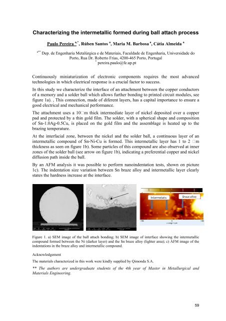
In this study we characterize the interface of an attachment between the copper conductors<br />
of a memory and a solder ball which allows further bonding to printed circuit modules, see<br />
figure 1a). , This connection, made of diferent layers, has a capital importance to ensure a<br />
good electrical and mechanical performance.<br />
The attachment uses a 10 m thick intermediate layer of nickel deposited over a copper<br />
pad and protected by a thin gold film. The solder, with a spherical shape and composition<br />
of Sn-1.0Ag-0.5Cu, is placed on the gold film and the assemblage is heated up to the<br />
brazing temperature.<br />
At the interfacial zone, between the nickel and the solder ball, a continuous layer of an<br />
intermetallic compound of Sn-Ni-Cu is formed. This intermetallic layer has 1 to 2 m<br />
thickness as seen on figure 1b). Some particles of this compound are also observed at inner<br />
zones of the solder ball (see arrow on figure 1b), indicating a preferential copper and nickel<br />
diffusion path inside the ball.<br />
By an AFM analysis it was possible to perform nanoindentation tests, shown on picture<br />
1c). The indentation size variation between Sn braze alloy and intermetallic layer clearly<br />
states the hardness increase at the interface.<br />
Figure 1. a) SEM image of the ball attach bonding; b) SEM image of interface showing the intermetallic<br />
compound formed between the Ni (darker layer) and the Sn braze alloy (lighter area); c) AFM image of the<br />
indentations in the braze alloy and intermetallic compound.<br />
Acknowledgement<br />
The materials characterized in this work were kindly supplied by Qimonda S.A.<br />
** The authors are undergraduate students of the 4th year of Master in Metallurgical and<br />
Materials Engineering.<br />
59