Workshopband als PDF - Mpc.belwue.de
Workshopband als PDF - Mpc.belwue.de
Workshopband als PDF - Mpc.belwue.de

Sie wollen auch ein ePaper? Erhöhen Sie die Reichweite Ihrer Titel.
YUMPU macht aus Druck-PDFs automatisch weboptimierte ePaper, die Google liebt.
MPC-WORKSHOP FEBRUAR 2013<br />
Design and Implementation of a Mixed-Signal ASIC in<br />
Ultra-Thin CMOS Technology for 2-D Stress<br />
Measurement<br />
Abstract—A CMOS sensor for in-plane stress<br />
measurement is presented. The <strong>de</strong>vice is <strong>de</strong>signed<br />
using the IMS 0.5 µm CMOS Gate Array technology<br />
and it is to be fabricated as a flexible chip using<br />
the Chipfilm TM technology of IMS CHIPS. The<br />
sensor consists of four channels, each of which<br />
inclu<strong>de</strong>s a sensor core, a readout circuit, and a 10bit<br />
analog-to-digital converter (ADC). The linearity<br />
of the sensor is enhanced by the <strong>de</strong>sign of the sensor<br />
core and readout. The readout is <strong>de</strong>signed to be<br />
insensitive to the induced stress in or<strong>de</strong>r to maintain<br />
proper operation at all times. The internal<br />
sensor timing can be tuned through a serial interface<br />
for adjusting the analog performance of the<br />
sensor.<br />
In<strong>de</strong>x Terms—Stress sensor, ultra-thin chip, flexible<br />
chip, stress-insensitive mixed-signal <strong>de</strong>sign<br />
I. INTRODUCTION<br />
Flexible electronics is a contemporary technology<br />
that is likely to grow rapidly in near future. The hybrid<br />
system-in-foil (SiF) <strong>de</strong>vices, that house an ultra-thin<br />
chip, are expected to be an important part of the market<br />
[1]. By using the properties of the ultra-thin chips,<br />
stress on a surface can be measured or topological<br />
information can be acquired from the adjacent surface.<br />
The piezoresistive effect in silicon is a well explained<br />
phenomenon which is wi<strong>de</strong>ly used for stress<br />
sensing. Resistors or MOSFET’s are used as sensing<br />
elements. The information is obtained by measuring<br />
the stress induced variation in resistance and mobility<br />
for resistors and MOSFET’s respectively. The choice<br />
differs according to the final application of the sensor.<br />
In literature, a number of studies are available and the<br />
target applications cover various topics such as <strong>de</strong>ntal<br />
care, wire bonding, flip chip bonding, and wafer stability<br />
[2]-[6].<br />
In this work, a sensor is <strong>de</strong>signed for measuring the<br />
in-plane stress or the flex on a bendable surface. Due<br />
to the extremely low thickness of the <strong>de</strong>vice, the rigid-<br />
Yigit U. Mahsereci, mahsereci@ims-chips.<strong>de</strong>, and Cor Scherjon,<br />
scherjon@ims-chips.<strong>de</strong> are with Institut für Mikroelektronik<br />
Stuttgart, Allmandring 30a, 70569 Stuttgart.<br />
Yigit U. Mahsereci, Cor Scherjon<br />
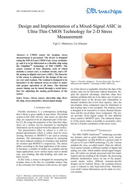
Figure 1: Ultra-thin (thickness < 20 µm) silicon chip. The chip is<br />
fabricated with Chipfilm TM technology of IMS CHIPS [10].<br />
ity of the silicon is negligible; therefore the data of the<br />
surface state can be harvested without distortion. Despite<br />
the physical advantage, ultra-thin chips have<br />
intrinsic problems that are to be taken care of such as,<br />
substantial stress in the <strong>de</strong>vices and vulnerability to<br />
thermal variations due to low heat capacity. Also, the<br />
out-of-plane stress component must be eliminated so<br />
that in-plane data is not corrupted. The readout circuit<br />
is <strong>de</strong>signed to be insensitive to stress, thermal fluctuations<br />
and the out-of-plane stress component. The sensor<br />
provi<strong>de</strong>s 10-bit digital output for four different<br />
stress sensitive MOSFET pairs. The enhanced linearity<br />
of the sensor makes it possible to accurately calculate<br />
the 2-D polar coordinates of the stress vector.<br />
II. GATEFOREST TM TECHNOLOGY<br />
The IMS CHIPS GateForest TM technology provi<strong>de</strong>s<br />
key features such as quick fabrication cycle, mixedsignal<br />
integration, on-chip RAMs at a process no<strong>de</strong> of<br />
0.8 µm or 0.5 µm CMOS technology [7], [8]. Various<br />
standard die sizes, so-called master chips are offered.<br />
Each master inclu<strong>de</strong>s a different number of digital and<br />
analog core cells, which enables mixed-signal integration.<br />
All wafers are already processed until the metallization<br />
and are residing in the foundry. By processing<br />
different metallization layers on top of the preprocessed<br />
master wafers, different customer-specific<br />
<strong>de</strong>signs can be realized. Hence, the complete process<br />
cycle is reduced to only back-end-of-line. Therefore,<br />
even small volume fabrications can be ma<strong>de</strong> in a lowcost<br />
manner.<br />
7
![[Geben Sie hier die Überschrift ein] - MPC](https://img.yumpu.com/8654082/1/188x260/geben-sie-hier-die-uberschrift-ein-mpc.jpg?quality=85)