Workshopband als PDF - Mpc.belwue.de
Workshopband als PDF - Mpc.belwue.de
Workshopband als PDF - Mpc.belwue.de

Sie wollen auch ein ePaper? Erhöhen Sie die Reichweite Ihrer Titel.
YUMPU macht aus Druck-PDFs automatisch weboptimierte ePaper, die Google liebt.
MPC-WORKSHOP FEBRUAR 2013<br />
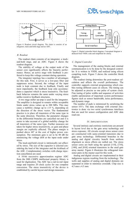
Figure 4: Readout circuit diagram. The chain is consists of an<br />
integrator, track-and-hold stage and an ADC.<br />
B. Readout<br />
The readout chain consists of an integrator, a trackand-hold<br />
stage, and an ADC. Figure 4 shows the<br />
readout diagram.<br />
The stability of voltage at the output no<strong>de</strong> of the<br />
sensor core significantly affects the linearity performance.<br />
Hence, an active stage with feedback is preferred<br />
to keep this voltage constant during operation.<br />
The integrator topology has a number of advantages<br />
for this task. First, it serves as a low-pass filter and<br />
suppresses noise. Second, the voltage of the input<br />
no<strong>de</strong> is kept constant due to feedback. Finally and<br />
most importantly, the feedback loop only accommodates<br />
a capacitor which is stress insensitive. The feedback<br />
behavior remains the same un<strong>de</strong>r varying stress<br />
unlike resistive feedback structures.<br />
A two stage miller op-amp is used for the integrator.<br />
The amplifier is <strong>de</strong>signed to remain within acceptable<br />
limits un<strong>de</strong>r stress values up to 200 MPa. This may<br />
cause a mobility change up to ±15 %, <strong>de</strong>pending on<br />
the direction of the stress vector. The fundamental<br />
practice is to place all transistors of the same type in<br />
the same direction. Therefore, the parameter changes<br />
in the differential branches are cancelled out and it is<br />
easier to take account of a global mobility change for<br />
all transistors of the same type. Further measures are<br />
taken for higher stress insensitivity, as gain and phase<br />
margin are explicitly affected. The phase margin is<br />
pushed above 60° at the cost of higher power consumption.<br />
The minimum gain is set to be 80 dB for<br />
minimizing the voltage drift at the input no<strong>de</strong> un<strong>de</strong>r<br />
stress.<br />
The track-and-hold circuit is intrinsically not affected<br />
by stress. The size of the capacitor is selected consi<strong>de</strong>ring<br />
the load of the integrator and the kickback of<br />
the ADC. Complementary switches with charge injection<br />
cancellation are used.<br />
A 10-bit successive approximation register ADC<br />
from the IMS CHIPS intellectual property library is<br />
used for digitization. The ADC has a rail-to-rail input<br />
range and requires 20 clock cycles for one complete<br />
conversion. The stress insensitivity of the <strong>de</strong>vice is<br />
established by careful layout and <strong>de</strong>sign measures.<br />
Figure 5: Digital controller block diagram. Conceptual diagram is<br />
<strong>de</strong>duced from VHDL co<strong>de</strong> and simplified for clarity.<br />
C. Digital Controller<br />
The management of the analog blocks and external<br />
communication is to be done by the <strong>de</strong>signed controller.<br />
It is written in VHDL and realized using silicon<br />
compiling tools. Figure 5 shows the controller block<br />
diagram.<br />
The readout timing <strong>de</strong>termines the post-readout calculation<br />
and affects the overall performance. The<br />
controller supports external programming which enables<br />
testing different cases on silicon. The timing can<br />
be adjusted as precise as one pulse of system clock.<br />
Fine tuning of pulse widths and sequence of activities<br />
enable optimization of important system performance<br />
figures such as sensor bandwidth, noise performance,<br />
and dynamic range.<br />
The number of pads is minimized by serializing the<br />
sensor I/O’s. The data exchange with external electronics<br />
is done via two serial synchronous interfaces<br />
that are used for sensor configuration and ADC data<br />
read-out.<br />
IV. IMPLEMENTATION<br />
Several intrinsic and extrinsic restrictions are present<br />
in layout level due to the gate array technology and<br />
stress exposure. All circuits except stress sensor cores<br />
are constructed with same-oriented transistors due to<br />
gate array technology. Differential branches in the<br />
analog and digital circuitry benefit from uniform<br />
alignment as stress effects are nulled out. The stress<br />
sensor cores are built using the special [110], [1¯10],<br />
[100], and [010] oriented transistors in the used gate<br />
array master. Figure 6 illustrates the orthogonal transistor<br />
pairs in the master used for this work.<br />
Analog and digital circuits are implemented in their<br />
indigenous regions resulting from the technology. The<br />
wells and supplies of analog and digital domains are<br />
separated in or<strong>de</strong>r to minimize crosstalk. Chip size is<br />
4.5 mm x 4.5 mm.<br />
9

![[Geben Sie hier die Überschrift ein] - MPC](https://img.yumpu.com/8654082/1/188x260/geben-sie-hier-die-uberschrift-ein-mpc.jpg?quality=85)