Workshopband als PDF - Mpc.belwue.de
Workshopband als PDF - Mpc.belwue.de
Workshopband als PDF - Mpc.belwue.de

Sie wollen auch ein ePaper? Erhöhen Sie die Reichweite Ihrer Titel.
YUMPU macht aus Druck-PDFs automatisch weboptimierte ePaper, die Google liebt.
MPC-WORKSHOP FEBRUAR 2013<br />
B. Adaptive Pulse Skipping -APS<br />
According to Fig. 2, path I and path II are used in<br />
buck mo<strong>de</strong> and path III and path IV are used in boost<br />
mo<strong>de</strong>. Besi<strong>de</strong>s, the sign<strong>als</strong> of the duty cycle D and its<br />
complement D’ are shown with the inductor current IL.<br />
Self-tuning pulse skipping (SPS) is utilized to extend<br />
the effective duty cycle. With the SPS, the duty cycle<br />
of the converter cannot be larger than 16.7 %. This<br />
value is large enough to ensure a smooth transition,<br />
when Vin comes close to Vout and not too large to unnecessarily<br />
enlarge the inductor current and output<br />
voltage ripple. But this limit slows down the charging<br />
or discharging performance of the inductor. If it would<br />
be possible to change the duty cycle to higher values,<br />
it could be <strong>als</strong>o possible to charge or discharge the<br />
inductor for a longer time. Thereby, the required<br />
charge in the inductor can be reached faster.<br />
To realize the adaptive duty cycle in case of load<br />
transition, the APS is used. To activate the APS a the<br />
feedback signal Vfb is compared to a higher and lower<br />
limit. If Vfb exceeds one of these limits the APS starts.<br />
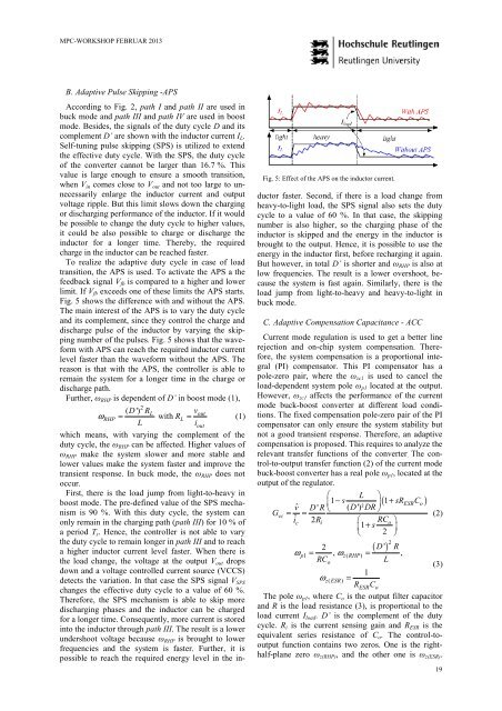
Fig. 5 shows the difference with and without the APS.<br />
The main interest of the APS is to vary the duty cycle<br />
and its complement, since they control the charge and<br />
discharge pulse of the inductor by varying the skipping<br />
number of the pulses. Fig. 5 shows that the waveform<br />
with APS can reach the required inductor current<br />
level faster than the waveform without the APS. The<br />
reason is that with the APS, the controller is able to<br />
remain the system for a longer time in the charge or<br />
discharge path.<br />
Further, ωRHP is <strong>de</strong>pen<strong>de</strong>nt of D’ in boost mo<strong>de</strong> (1),<br />
2<br />
( D ') RL<br />
vout<br />
ω RHP = with RL<br />
= (1)<br />
L i<br />
out<br />
which means, with varying the complement of the<br />
duty cycle, the ωRHP can be affected. Higher values of<br />
ωRHP make the system slower and more stable and<br />
lower values make the system faster and improve the<br />
transient response. In buck mo<strong>de</strong>, the ωRHP does not<br />
occur.<br />
First, there is the load jump from light-to-heavy in<br />
boost mo<strong>de</strong>. The pre-<strong>de</strong>fined value of the SPS mechanism<br />
is 90 %. With this duty cycle, the system can<br />
only remain in the charging path (path III) for 10 % of<br />
a period Ts. Hence, the controller is not able to vary<br />
the duty cycle to remain longer in path III and to reach<br />
a higher inductor current level faster. When there is<br />
the load change, the voltage at the output Vout drops<br />
down and a voltage controlled current source (VCCS)<br />
<strong>de</strong>tects the variation. In that case the SPS signal VSPS<br />
changes the effective duty cycle to a value of 60 %.<br />
Therefore, the SPS mechanism is able to skip more<br />
discharging phases and the inductor can be charged<br />
for a longer time. Consequently, more current is stored<br />
into the inductor through path III. The result is a lower<br />
un<strong>de</strong>rshoot voltage because ωRHP is brought to lower<br />
frequencies and the system is faster. Further, it is<br />
possible to reach the required energy level in the in-<br />
Fig. 5: Effect of the APS on the inductor current.<br />
ductor faster. Second, if there is a load change from<br />
heavy-to-light load, the SPS signal <strong>als</strong>o sets the duty<br />
cycle to a value of 60 %. In that case, the skipping<br />
number is <strong>als</strong>o higher, so the charging phase of the<br />
inductor is skipped and the energy in the inductor is<br />
brought to the output. Hence, it is possible to use the<br />
energy in the inductor first, before recharging it again.<br />
But however, in total D’ is shorter and ωRHP is <strong>als</strong>o at<br />
low frequencies. The result is a lower overshoot, because<br />
the system is fast again. Similarly, there is the<br />
load jump from light-to-heavy and heavy-to-light in<br />
buck mo<strong>de</strong>.<br />
C. Adaptive Compensation Capacitance - ACC<br />
Current mo<strong>de</strong> regulation is used to get a better line<br />
rejection and on-chip system compensation. Therefore,<br />
the system compensation is a proportional integral<br />
(PI) compensator. This PI compensator has a<br />
pole-zero pair, where the ωzc1 is used to cancel the<br />
load-<strong>de</strong>pen<strong>de</strong>nt system pole ωp1 located at the output.<br />
However, ωzc1 affects the performance of the current<br />
mo<strong>de</strong> buck-boost converter at different load conditions.<br />
The fixed compensation pole-zero pair of the PI<br />
compensator can only ensure the system stability but<br />
not a good transient response. Therefore, an adaptive<br />
compensation is proposed. This requires to analyze the<br />
relevant transfer functions of the converter. The control-to-output<br />
transfer function (2) of the current mo<strong>de</strong><br />
buck-boost converter has a real pole ωp1, located at the<br />
output of the regulator.<br />
G<br />
vc<br />
⎛ L ⎞<br />
⎜1− s ⎟ 1+<br />
sR C<br />
vˆ D ' R ( D ')² DR<br />
= =<br />
⎝ ⎠<br />
iˆ<br />
c 2Ri<br />
⎛ RCo<br />
⎞<br />
⎜1+ s<br />
2<br />
⎟<br />
⎝ ⎠<br />
p1 z( RHP)<br />
o<br />
( )<br />
( ) 2<br />
'<br />
2 D R<br />
ω = , ω = ,<br />
RC L<br />
ω<br />
1<br />
=<br />
R C<br />
ESR o<br />
(2)<br />
(3)<br />
z( ESR)<br />
ESR o<br />
The pole ωp1, where Co is the output filter capacitor<br />
and R is the load resistance (3), is proportional to the<br />
load current Iload. D’ is the complement of the duty<br />
cycle. Ri is the current sensing gain and RESR is the<br />
equivalent series resistance of Co. The control-tooutput<br />
function contains two zeros. One is the righthalf-plane<br />
zero ωz(RHP), and the other one is ωz(ESR).<br />
19


![[Geben Sie hier die Überschrift ein] - MPC](https://img.yumpu.com/8654082/1/188x260/geben-sie-hier-die-uberschrift-ein-mpc.jpg?quality=85)