

Full-Custom Layout of an SRAM-Based FPGA - University of Toronto
Full-Custom Layout of an SRAM-Based FPGA - University of Toronto
Full-Custom Layout of an SRAM-Based FPGA - University of Toronto

Create successful ePaper yourself
Turn your PDF publications into a flip-book with our unique Google optimized e-Paper software.
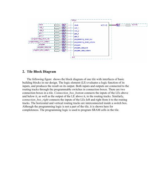
2. Tile Block Diagram<br />
The following figure shows the block diagram <strong>of</strong> one tile with interfaces <strong>of</strong> basic<br />
building blocks in our design. The logic element (LE) evaluates a logic function <strong>of</strong> its<br />
inputs, <strong>an</strong>d produces the result on its output. Both inputs <strong>an</strong>d outputs are connected to the<br />
routing tracks through the programmable switches in connection boxes. There are two<br />
connection boxes in a tile. Connection_box_bottom connects the inputs <strong>of</strong> the LEs above<br />
<strong>an</strong>d below it, as well as the output <strong>of</strong> the LE above it, to the routing tracks. Similarly,<br />
connection_box_right connects the inputs <strong>of</strong> the LEs left <strong>an</strong>d right from it to the routing<br />
tracks. The horizontal <strong>an</strong>d vertical routing tracks are interconnected inside a switch box.<br />
Although the programming logic is not a part <strong>of</strong> the tile, it is shown here for<br />
completeness. The programming logic is used to program <strong>SRAM</strong> cells in the tile.


