

Full-Custom Layout of an SRAM-Based FPGA - University of Toronto
Full-Custom Layout of an SRAM-Based FPGA - University of Toronto
Full-Custom Layout of an SRAM-Based FPGA - University of Toronto

Create successful ePaper yourself
Turn your PDF publications into a flip-book with our unique Google optimized e-Paper software.
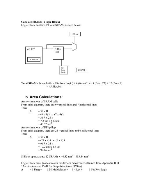
Caculate <strong>SRAM</strong>s in logic Block:<br />
Logic Block contains 19 total <strong>SRAM</strong>s as seen below:<br />
4 LUT<br />
16 <strong>SRAM</strong>S<br />
D Flip<br />
Flop<br />
Set<br />
Reset<br />
Logic<br />
1 <strong>SRAM</strong><br />
2 <strong>SRAM</strong><br />
Total <strong>SRAM</strong>s for each tile = 19 (from Logic) + 6 (from C1) + 8 (from C2) + 12 (from S)<br />
= 45 <strong>SRAM</strong>s<br />
b. Area Calculations:<br />
Area estimations <strong>of</strong> <strong>SRAM</strong> cells<br />
From stick diagram, there are 9 vertical lines <strong>an</strong>d 7 horizontal lines<br />
Thus:<br />
A = W x H<br />
= (9 x 4) λ x (7 x 4) λ<br />
= 36 λ x 28 λ<br />
= 7.2 um x 5.6 um<br />
= 40.32 um 2<br />
Area estimations <strong>of</strong> DFlipFlop<br />
From stick diagram, there are 24 vertical lines <strong>an</strong>d 6 horizontal lines<br />
Thus<br />
A = W x H<br />
= (24 x 4) λ x (6 x 4) λ<br />
= 96 λ x 24 λ<br />
= 19.2 um x 4.8 um<br />
= 92.16 um 2<br />
S Block approx area: 12 <strong>SRAM</strong>s x 40.32 um 2 = 483.84 um 2<br />
Logic Block area: (not estimates for devices below were obtained from Appendix B <strong>of</strong><br />
“Architecture <strong>an</strong>d CAD for Deep-Submicron <strong>FPGA</strong>s)<br />
A = 1 Dreg + 1 2-1Multiplexer + 1 4 Lut + 1 Set/Rest logic


