

Full-Custom Layout of an SRAM-Based FPGA - University of Toronto
Full-Custom Layout of an SRAM-Based FPGA - University of Toronto
Full-Custom Layout of an SRAM-Based FPGA - University of Toronto

You also want an ePaper? Increase the reach of your titles
YUMPU automatically turns print PDFs into web optimized ePapers that Google loves.
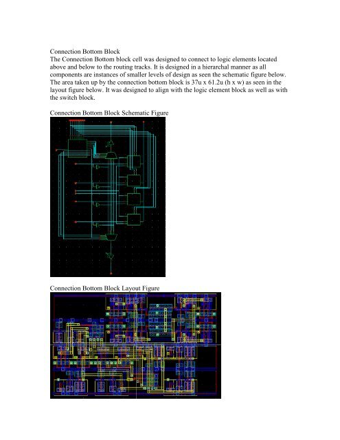
Connection Bottom Block<br />
The Connection Bottom block cell was designed to connect to logic elements located<br />
above <strong>an</strong>d below to the routing tracks. It is designed in a hierarchal m<strong>an</strong>ner as all<br />
components are inst<strong>an</strong>ces <strong>of</strong> smaller levels <strong>of</strong> design as seen the schematic figure below.<br />
The area taken up by the connection bottom block is 37u x 61.2u (h x w) as seen in the<br />
layout figure below. It was designed to align with the logic element block as well as with<br />
the switch block.<br />
Connection Bottom Block Schematic Figure<br />
Connection Bottom Block <strong>Layout</strong> Figure


