

Full-Custom Layout of an SRAM-Based FPGA - University of Toronto
Full-Custom Layout of an SRAM-Based FPGA - University of Toronto
Full-Custom Layout of an SRAM-Based FPGA - University of Toronto

You also want an ePaper? Increase the reach of your titles
YUMPU automatically turns print PDFs into web optimized ePapers that Google loves.
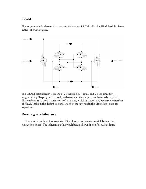
<strong>SRAM</strong><br />
The programmable elements in our architecture are <strong>SRAM</strong> cells. An <strong>SRAM</strong> cell is shown<br />
in the following figure.<br />
The <strong>SRAM</strong> cell basically consists <strong>of</strong> 2 coupled NOT gates, <strong>an</strong>d 2 pass gates for<br />
programming. To program the cell, both data <strong>an</strong>d its complement have to be applied.<br />
This enables us to use all tr<strong>an</strong>sistors <strong>of</strong> unit size, which is import<strong>an</strong>t, because the number<br />
<strong>of</strong> <strong>SRAM</strong> cells in the design is large, <strong>an</strong>d thus the savings in the <strong>SRAM</strong> cell area are<br />
import<strong>an</strong>t.<br />
Routing Architecture<br />
The routing architecture consists <strong>of</strong> two basic components: switch boxes, <strong>an</strong>d<br />
connection boxes. The schematic <strong>of</strong> a switch box is shown in the following figure


