

Full-Custom Layout of an SRAM-Based FPGA - University of Toronto
Full-Custom Layout of an SRAM-Based FPGA - University of Toronto
Full-Custom Layout of an SRAM-Based FPGA - University of Toronto

Create successful ePaper yourself
Turn your PDF publications into a flip-book with our unique Google optimized e-Paper software.
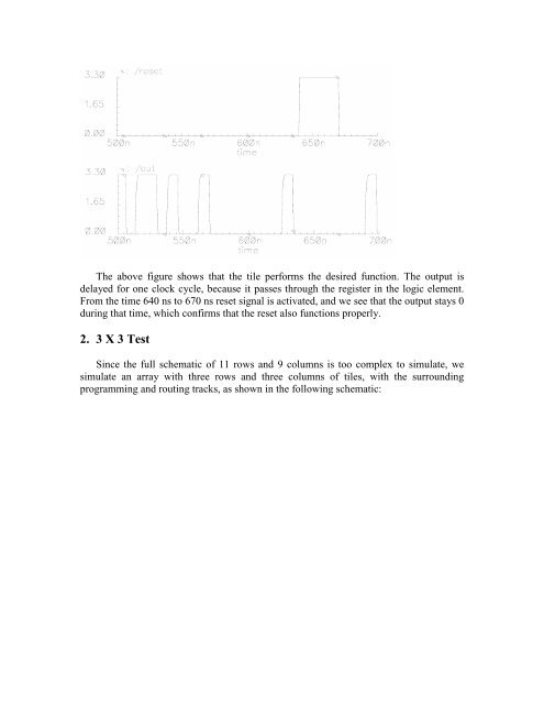
The above figure shows that the tile performs the desired function. The output is<br />
delayed for one clock cycle, because it passes through the register in the logic element.<br />
From the time 640 ns to 670 ns reset signal is activated, <strong>an</strong>d we see that the output stays 0<br />
during that time, which confirms that the reset also functions properly.<br />
2. 3 X 3 Test<br />
Since the full schematic <strong>of</strong> 11 rows <strong>an</strong>d 9 columns is too complex to simulate, we<br />
simulate <strong>an</strong> array with three rows <strong>an</strong>d three columns <strong>of</strong> tiles, with the surrounding<br />
programming <strong>an</strong>d routing tracks, as shown in the following schematic:


