

Full-Custom Layout of an SRAM-Based FPGA - University of Toronto
Full-Custom Layout of an SRAM-Based FPGA - University of Toronto
Full-Custom Layout of an SRAM-Based FPGA - University of Toronto

You also want an ePaper? Increase the reach of your titles
YUMPU automatically turns print PDFs into web optimized ePapers that Google loves.
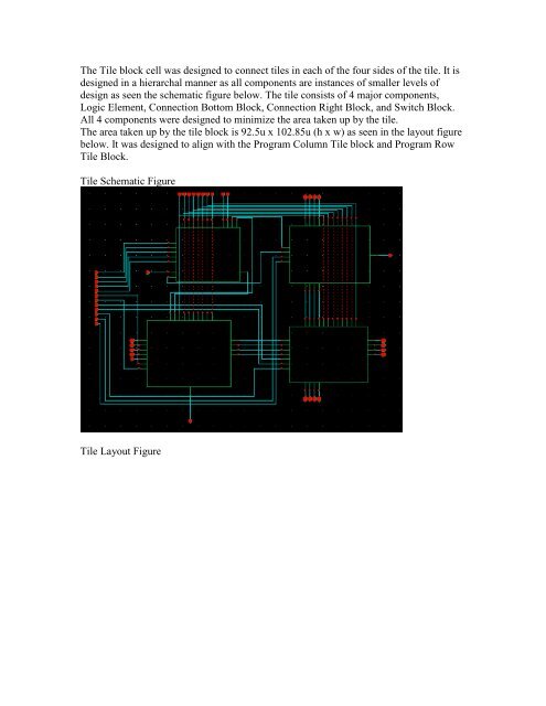
The Tile block cell was designed to connect tiles in each <strong>of</strong> the four sides <strong>of</strong> the tile. It is<br />
designed in a hierarchal m<strong>an</strong>ner as all components are inst<strong>an</strong>ces <strong>of</strong> smaller levels <strong>of</strong><br />
design as seen the schematic figure below. The tile consists <strong>of</strong> 4 major components,<br />
Logic Element, Connection Bottom Block, Connection Right Block, <strong>an</strong>d Switch Block.<br />
All 4 components were designed to minimize the area taken up by the tile.<br />
The area taken up by the tile block is 92.5u x 102.85u (h x w) as seen in the layout figure<br />
below. It was designed to align with the Program Column Tile block <strong>an</strong>d Program Row<br />
Tile Block.<br />
Tile Schematic Figure<br />
Tile <strong>Layout</strong> Figure


