

Full-Custom Layout of an SRAM-Based FPGA - University of Toronto
Full-Custom Layout of an SRAM-Based FPGA - University of Toronto
Full-Custom Layout of an SRAM-Based FPGA - University of Toronto

Create successful ePaper yourself
Turn your PDF publications into a flip-book with our unique Google optimized e-Paper software.
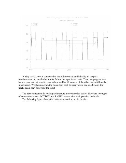
Wiring track L is connected to the pulse source, <strong>an</strong>d initially all the pass<br />
tr<strong>an</strong>sistors are on, so all other tracks follow the input from L. Then, we program one<br />
by one pass tr<strong>an</strong>sistor not to pass values, <strong>an</strong>d by 30 ns none <strong>of</strong> the other tracks follow the<br />
input signal. We then program the tr<strong>an</strong>sistors back to pass values, <strong>an</strong>d one by one, the<br />
tracks again start following the input.<br />
The next component in routing architecture are connection boxes. There are two types<br />
<strong>of</strong> connection boxes: BOTTOM <strong>an</strong>d RIGHT, named after their position in the tile.<br />
The following figure shows the bottom connection box in the tile.


