

Full-Custom Layout of an SRAM-Based FPGA - University of Toronto
Full-Custom Layout of an SRAM-Based FPGA - University of Toronto
Full-Custom Layout of an SRAM-Based FPGA - University of Toronto

You also want an ePaper? Increase the reach of your titles
YUMPU automatically turns print PDFs into web optimized ePapers that Google loves.
1. <strong>FPGA</strong> Design<br />
The purpose <strong>of</strong> this project is to implement a full custom layout <strong>of</strong> a simple <strong>FPGA</strong><br />
device. The basic building block <strong>of</strong> <strong>an</strong> <strong>FPGA</strong> is logic element (LE), which consists <strong>of</strong> a<br />
lookup table (LUT), a flip-flop, <strong>an</strong>d a multiplexer that chooses whether to forward the<br />
output <strong>of</strong> the LUT or the flip-flop outside the LE. A k-LUT consist <strong>of</strong> a set <strong>of</strong><br />
multiplexers that implement <strong>an</strong>y function <strong>of</strong> k inputs by forwarding one <strong>of</strong> the 2 k<br />
configuration bits to the output <strong>of</strong> the LUT. LEs are interconnected with routing<br />
resources which are also configurable. Configuration <strong>of</strong> routing resources is achieved<br />
using pass gates controlled by a routing configuration bits. The desired configuration is<br />
stored in the <strong>SRAM</strong> cells. One <strong>SRAM</strong> cell is required per pass gate, while a k-LUT<br />
requires 2 k <strong>SRAM</strong> cells.<br />
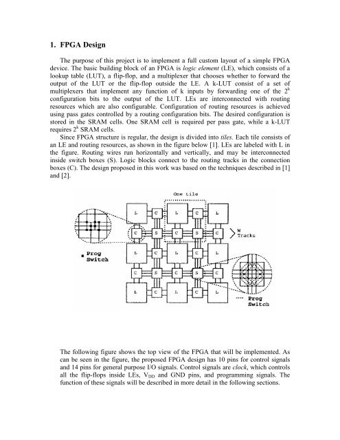
Since <strong>FPGA</strong> structure is regular, the design is divided into tiles. Each tile consists <strong>of</strong><br />
<strong>an</strong> LE <strong>an</strong>d routing resources, as shown in the figure below [1]. LEs are labeled with L in<br />
the figure. Routing wires run horizontally <strong>an</strong>d vertically, <strong>an</strong>d may be interconnected<br />
inside switch boxes (S). Logic blocks connect to the routing tracks in the connection<br />
boxes (C). The design proposed in this work was based on the techniques described in [1]<br />
<strong>an</strong>d [2].<br />
The following figure shows the top view <strong>of</strong> the <strong>FPGA</strong> that will be implemented. As<br />
c<strong>an</strong> be seen in the figure, the proposed <strong>FPGA</strong> design has 10 pins for control signals<br />
<strong>an</strong>d 14 pins for general purpose I/O signals. Control signals are clock, which controls<br />
all the flip-flops inside LEs, VDD <strong>an</strong>d GND pins, <strong>an</strong>d programming signals. The<br />
function <strong>of</strong> these signals will be described in more detail in the following sections.


