

Full-Custom Layout of an SRAM-Based FPGA - University of Toronto
Full-Custom Layout of an SRAM-Based FPGA - University of Toronto
Full-Custom Layout of an SRAM-Based FPGA - University of Toronto

You also want an ePaper? Increase the reach of your titles
YUMPU automatically turns print PDFs into web optimized ePapers that Google loves.
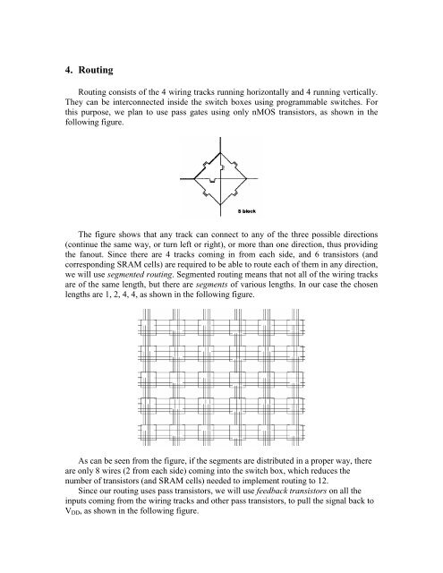
4. Routing<br />
Routing consists <strong>of</strong> the 4 wiring tracks running horizontally <strong>an</strong>d 4 running vertically.<br />
They c<strong>an</strong> be interconnected inside the switch boxes using programmable switches. For<br />
this purpose, we pl<strong>an</strong> to use pass gates using only nMOS tr<strong>an</strong>sistors, as shown in the<br />
following figure.<br />
The figure shows that <strong>an</strong>y track c<strong>an</strong> connect to <strong>an</strong>y <strong>of</strong> the three possible directions<br />
(continue the same way, or turn left or right), or more th<strong>an</strong> one direction, thus providing<br />
the f<strong>an</strong>out. Since there are 4 tracks coming in from each side, <strong>an</strong>d 6 tr<strong>an</strong>sistors (<strong>an</strong>d<br />
corresponding <strong>SRAM</strong> cells) are required to be able to route each <strong>of</strong> them in <strong>an</strong>y direction,<br />
we will use segmented routing. Segmented routing me<strong>an</strong>s that not all <strong>of</strong> the wiring tracks<br />
are <strong>of</strong> the same length, but there are segments <strong>of</strong> various lengths. In our case the chosen<br />
lengths are 1, 2, 4, 4, as shown in the following figure.<br />
As c<strong>an</strong> be seen from the figure, if the segments are distributed in a proper way, there<br />
are only 8 wires (2 from each side) coming into the switch box, which reduces the<br />
number <strong>of</strong> tr<strong>an</strong>sistors (<strong>an</strong>d <strong>SRAM</strong> cells) needed to implement routing to 12.<br />
Since our routing uses pass tr<strong>an</strong>sistors, we will use feedback tr<strong>an</strong>sistors on all the<br />
inputs coming from the wiring tracks <strong>an</strong>d other pass tr<strong>an</strong>sistors, to pull the signal back to<br />
VDD, as shown in the following figure.


