

Full-Custom Layout of an SRAM-Based FPGA - University of Toronto
Full-Custom Layout of an SRAM-Based FPGA - University of Toronto
Full-Custom Layout of an SRAM-Based FPGA - University of Toronto

You also want an ePaper? Increase the reach of your titles
YUMPU automatically turns print PDFs into web optimized ePapers that Google loves.
1. Introduction<br />
The goal <strong>of</strong> this project was to design <strong>an</strong> <strong>SRAM</strong>-based Field Programmable Gate Array (<strong>FPGA</strong>), <strong>an</strong>d<br />
implement it by laying it out as a full-custom design in 0.35μ TSMC process. The design was limited by<br />
maximal area <strong>of</strong> 4 mm 2 <strong>an</strong>d by the time available for the design process (6 weeks).<br />
The tasks necessary to build <strong>an</strong>d verify <strong>an</strong> <strong>FPGA</strong> include system level pl<strong>an</strong>ning, schematic design, cell<br />
layout, <strong>an</strong>d final chip layout. These steps are described in more detail in the following sections.<br />
2. System Outline<br />
On the highest level, <strong>an</strong> <strong>FPGA</strong> consists <strong>of</strong> programmable logic elements <strong>an</strong>d programmable routing<br />
resources used to interconnect the logic elements. The logic elements implement the combinational <strong>an</strong>d<br />
sequential logic functions the user w<strong>an</strong>ts to implement in the <strong>FPGA</strong>, <strong>an</strong>d the routing resources interconnect<br />
logic elements to implement the desired system. <strong>FPGA</strong> design usually consists <strong>of</strong> <strong>an</strong> array <strong>of</strong> identical<br />
blocks <strong>of</strong> logic <strong>an</strong>d routing resources called tiles. The structure <strong>of</strong> the tile with the corresponding<br />
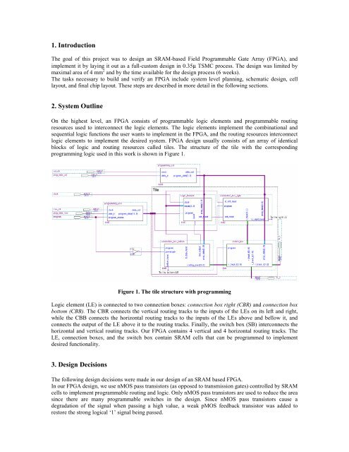
programming logic used in this work is shown in Figure 1.<br />
Figure 1. The tile structure with programming<br />
Logic element (LE) is connected to two connection boxes: connection box right (CBR) <strong>an</strong>d connection box<br />
bottom (CBB). The CBR connects the vertical routing tracks to the inputs <strong>of</strong> the LEs on its left <strong>an</strong>d right,<br />
while the CBB connects the horizontal routing tracks to the inputs <strong>of</strong> the LEs above <strong>an</strong>d bellow it, <strong>an</strong>d<br />
connects the output <strong>of</strong> the LE above it to the routing tracks. Finally, the switch box (SB) interconnects the<br />
horizontal <strong>an</strong>d vertical routing tracks. Our <strong>FPGA</strong> contains 4 vertical <strong>an</strong>d 4 horizontal routing tracks. The<br />
LE, connection boxes, <strong>an</strong>d the switch box contain <strong>SRAM</strong> cells that c<strong>an</strong> be programmed to implement<br />
desired functionality.<br />
3. Design Decisions<br />
The following design decisions were made in our design <strong>of</strong> <strong>an</strong> <strong>SRAM</strong> based <strong>FPGA</strong>.<br />
In our <strong>FPGA</strong> design, we use nMOS pass tr<strong>an</strong>sistors (as opposed to tr<strong>an</strong>smission gates) controlled by <strong>SRAM</strong><br />
cells to implement programmable routing <strong>an</strong>d logic. Only nMOS pass tr<strong>an</strong>sistors are used to reduce the area<br />
since there are m<strong>an</strong>y programmable switches in the design. Since nMOS pass tr<strong>an</strong>sistors cause a<br />
degradation <strong>of</strong> the signal when passing a high value, a weak pMOS feedback tr<strong>an</strong>sistor was added to<br />
restore the strong logical ‘1’ signal being passed.


