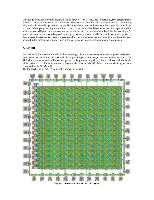
Our design contains 240 tiles org<strong>an</strong>ized in <strong>an</strong> array <strong>of</strong> 16x15 tiles, <strong>an</strong>d contains 10,800 programmable elements. To test the whole device, we would need to determine the state <strong>of</strong> each <strong>of</strong> those programming bits, which is normally performed by <strong>an</strong> <strong>FPGA</strong> synthesis tool, <strong>an</strong>d then run the simulation with input sequence <strong>of</strong> the programming bits <strong>an</strong>d test vectors. Since such a simulation overcomes the capacities <strong>of</strong> the available tools (HSpice), <strong>an</strong>d requires excessive amount <strong>of</strong> time, we have simulated the functionality <strong>of</strong> a single tile with the corresponding routing <strong>an</strong>d programming resources. All the simulation results produced the expected behaviour, <strong>an</strong>d since we have tested all the components in our system in a configuration they are used in the system, we consider this a sufficient pro<strong>of</strong> <strong>of</strong> the correct functionality <strong>of</strong> our design. 5. <strong>Layout</strong> We designed all our basic cells to have the same height. This was necessary to match the power <strong>an</strong>d ground lines when the cells abut. The cell with the largest height in our design was <strong>an</strong> inverter <strong>of</strong> size 2. The <strong>SRAM</strong> was the most used cell in our design <strong>an</strong>d its height was only slightly increased to match the height <strong>of</strong> the inverter cell. This allowed us to decrease the width <strong>of</strong> the <strong>SRAM</strong> cell thus minimizing the area consumed by the <strong>SRAM</strong> cell. The top level view <strong>of</strong> the <strong>FPGA</strong> layout is shown in Figure 3. Figure 3. Top-level view <strong>of</strong> the chip layout
The final design contains 48 pins. The number <strong>of</strong> pins was limited by the number <strong>of</strong> pads that c<strong>an</strong> fit on a die <strong>of</strong> size 2x2 mm. 38 pins are dedicated for general purpose input <strong>an</strong>d output, while the remaining 10 pins are used for power supply (2 pins), ground (2 pins), programming (5 pins), <strong>an</strong>d global clock, which is distributed to the flip-flops in all LEs in the device. The global clock is distributed by <strong>an</strong> H-tree structure inside the device to provide the low-skew clock. 6. Conclusions <strong>an</strong>d Future Work Our final design passes all DRC checks, <strong>an</strong>d LVS shows that the netlist matches our schematic. Currently, this project fully implements <strong>an</strong> <strong>FPGA</strong>, but some future work may be beneficial. The areas that should be covered by future work include simulation, power distribution network, <strong>an</strong>d I/O pads. Firstly, we were able to simulate the full tile with programming using HSpice, but no larger designs. To simulate the whole design, we would like to use <strong>an</strong>other tool, such as N<strong>an</strong>oSim, that is known to have been used for simulation by other researchers that have fabricated <strong>FPGA</strong>s. Another choice is to use a hybrid VHDL/Verilog <strong>an</strong>d schematic simulation in Cadence, which could also reduce simulation time <strong>an</strong>d complexity. Secondly, the power distribution grid, could be improved. Although our power distribution lines are comparable to other <strong>FPGA</strong> designs used in research, there is some concern that the metal lines are too narrow. Since the design is very regular, the cells could be spaced further apart to allow for wider metal lines, which should be done before the tapeout. Another area for improvement is the use <strong>of</strong> I/O pads. In the current implementation, all general pins are set to be either inputs or outputs. Generally, most <strong>FPGA</strong>s allow all general purpose pins to be programmed to be either inputs or outputs, which requires <strong>an</strong> extra <strong>SRAM</strong> cell. This was not done in the current implementation, because the provided pad library does not contain I/O pads. Finally, more adv<strong>an</strong>ced features, such as memory resources, PLL blocks, DSP blocks, carry-chains, could be added to the design. This would make the design usable in a wide variety <strong>of</strong> applications. 7. Division <strong>of</strong> Tasks Blair Fort: LUT (pl<strong>an</strong>ning, schematic, simulation, layout, DRC, LVS), Logic element (pl<strong>an</strong>ning, schematic, simulation, layout, DRC, LVS), connection boxes (layout, DRC, LVS), parts <strong>of</strong> reports <strong>an</strong>d presentations D<strong>an</strong>iele Paladino: Area estimation for the whole design, <strong>SRAM</strong> (pl<strong>an</strong>ning, schematic, simulation, layout, DRC, LVS), shift registers (pl<strong>an</strong>ning, schematic, simulation, layout, DRC, LVS), programming logic (pl<strong>an</strong>ning, schematic, simulation, layout, DRC, LVS), parts <strong>of</strong> reports <strong>an</strong>d presentations Fr<strong>an</strong>jo Plavec: connection boxes (pl<strong>an</strong>ning, schematic, simulation), switch box (pl<strong>an</strong>ning, schematic, simulation, layout, DRC, LVS), top-level (schematic, simulation, layout, DRC, LVS), parts <strong>of</strong> reports <strong>an</strong>d presentations