

Full-Custom Layout of an SRAM-Based FPGA - University of Toronto
Full-Custom Layout of an SRAM-Based FPGA - University of Toronto
Full-Custom Layout of an SRAM-Based FPGA - University of Toronto

Create successful ePaper yourself
Turn your PDF publications into a flip-book with our unique Google optimized e-Paper software.
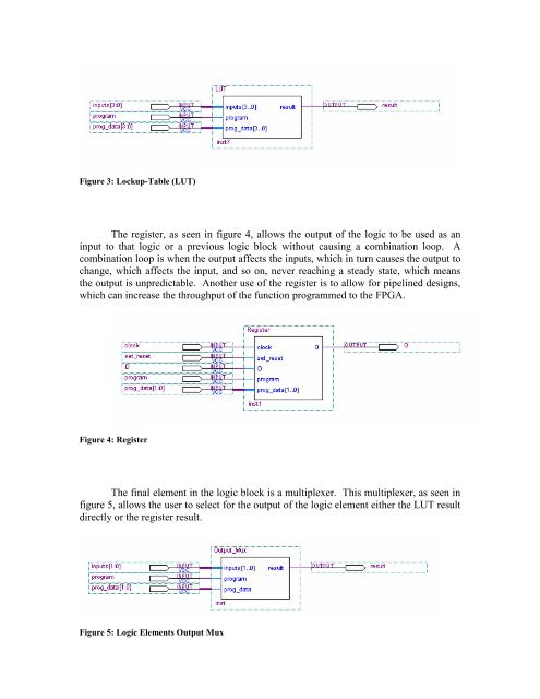
Figure 3: Lockup-Table (LUT)<br />
The register, as seen in figure 4, allows the output <strong>of</strong> the logic to be used as <strong>an</strong><br />
input to that logic or a previous logic block without causing a combination loop. A<br />
combination loop is when the output affects the inputs, which in turn causes the output to<br />
ch<strong>an</strong>ge, which affects the input, <strong>an</strong>d so on, never reaching a steady state, which me<strong>an</strong>s<br />
the output is unpredictable. Another use <strong>of</strong> the register is to allow for pipelined designs,<br />
which c<strong>an</strong> increase the throughput <strong>of</strong> the function programmed to the <strong>FPGA</strong>.<br />
Figure 4: Register<br />
The final element in the logic block is a multiplexer. This multiplexer, as seen in<br />
figure 5, allows the user to select for the output <strong>of</strong> the logic element either the LUT result<br />
directly or the register result.<br />
Figure 5: Logic Elements Output Mux


