

Full-Custom Layout of an SRAM-Based FPGA - University of Toronto
Full-Custom Layout of an SRAM-Based FPGA - University of Toronto
Full-Custom Layout of an SRAM-Based FPGA - University of Toronto

You also want an ePaper? Increase the reach of your titles
YUMPU automatically turns print PDFs into web optimized ePapers that Google loves.
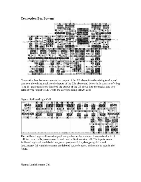
Connection Box Bottom<br />
Connection box bottom connects the output <strong>of</strong> the LE above it to the wiring tracks, <strong>an</strong>d<br />
connects the wiring tracks to the inputs <strong>of</strong> the LEs above <strong>an</strong>d below it. It consists <strong>of</strong> 4 big<br />
(size 10) pass tr<strong>an</strong>sistors that feed the output <strong>of</strong> the LE above it to the tracks, <strong>an</strong>d two<br />
cells <strong>of</strong> type “input to LE”, with the corresponding <strong>SRAM</strong> cells<br />
Figure: SetResetLogic Cell<br />
The SetResetLogic cell was designed using a hierarchal m<strong>an</strong>ner. It consists <strong>of</strong> a XOR<br />
cell, two n<strong>an</strong>d cells, two sram cells <strong>an</strong>d two buffer&inverter cell. The inputs to our<br />
SetResetLogic cell are labeled set_reset, program, data_prog <strong>an</strong>d<br />
data_progb <strong>an</strong>d the outputs are labeled set, setb, reset, <strong>an</strong>d resetb as seen in the<br />
figure.<br />
Figure: LogicElement Cell


