

Configuration and Remote System Upgrades in Cyclone IV ... - Altera
Configuration and Remote System Upgrades in Cyclone IV ... - Altera
Configuration and Remote System Upgrades in Cyclone IV ... - Altera

You also want an ePaper? Increase the reach of your titles
YUMPU automatically turns print PDFs into web optimized ePapers that Google loves.
8–16 Chapter 8: <strong>Configuration</strong> <strong>and</strong> <strong>Remote</strong> <strong>System</strong> <strong>Upgrades</strong> <strong>in</strong> <strong>Cyclone</strong> <strong>IV</strong> Devices<br />
<strong>Configuration</strong><br />
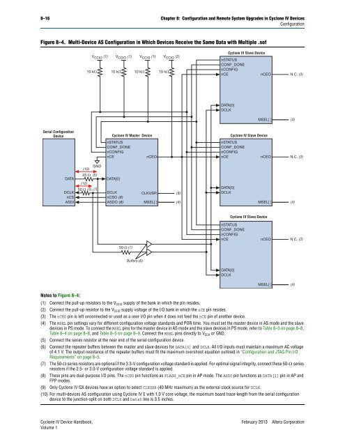
Figure 8–4. Multi-Device AS <strong>Configuration</strong> <strong>in</strong> Which Devices Receive the Same Data with Multiple .sof<br />
Serial <strong>Configuration</strong><br />
Device<br />
DATA<br />
DCLK<br />
nCS<br />
ASDI<br />
Notes to Figure 8–4:<br />
(10)<br />
V CCIO (1) V CCIO (1)<br />
GND<br />
nSTATUS<br />
CONF_DONE<br />
nCONFIG<br />
nCE<br />
DATA[0]<br />
DCLK<br />
nCSO (8)<br />
ASDO (8)<br />
V CCIO (1) V CCIO (2)<br />
10 kΩ 10 kΩ 10 kΩ 10 kΩ<br />
25 Ω (5)<br />
(10)<br />
50 Ω (5), (7)<br />
<strong>Cyclone</strong> <strong>IV</strong> Master Device<br />
50 Ω (7)<br />
Buffers (6)<br />
nCEO<br />
CLKUSR (9)<br />
MSEL[ ]<br />
nSTATUS<br />
CONF_DONE<br />
nCONFIG<br />
nCE<br />
DATA[0]<br />
DCLK<br />
<strong>Cyclone</strong> <strong>IV</strong> Slave Device<br />
nSTATUS<br />
CONF_DONE<br />
nCONFIG<br />
nCE<br />
DATA[0]<br />
DCLK<br />
(4) MSEL[ ]<br />
nSTATUS<br />
CONF_DONE<br />
nCONFIG<br />
nCE<br />
DATA[0]<br />
DCLK<br />
nCEO N.C. (3)<br />
MSEL[ ]<br />
<strong>Cyclone</strong> <strong>IV</strong> Slave Device<br />
<strong>Cyclone</strong> <strong>IV</strong> Slave Device<br />
(1) Connect the pull-up resistors to the VCCIO supply of the bank <strong>in</strong> which the p<strong>in</strong> resides.<br />
(2) Connect the pull-up resistor to the VCCIO supply voltage of the I/O bank <strong>in</strong> which the nCE p<strong>in</strong> resides.<br />
(3) The nCEO p<strong>in</strong> is left unconnected or used as a user I/O p<strong>in</strong> when it does not feed the nCE p<strong>in</strong> of another device.<br />
(4) The MSEL p<strong>in</strong> sett<strong>in</strong>gs vary for different configuration voltage st<strong>and</strong>ards <strong>and</strong> POR time. You must set the master device <strong>in</strong> AS mode <strong>and</strong> the slave<br />
devices <strong>in</strong> PS mode. To connect the MSEL p<strong>in</strong>s for the master device <strong>in</strong> AS mode <strong>and</strong> the slave devices <strong>in</strong> PS mode, refer to Table 8–3 on page 8–8,<br />
Table 8–4 on page 8–8, <strong>and</strong> Table 8–5 on page 8–9. Connect the MSEL p<strong>in</strong>s directly to VCCA or GND.<br />
(5) Connect the series resistor at the near end of the serial configuration device.<br />
(6) Connect the repeater buffers between the master <strong>and</strong> slave devices for DATA[0] <strong>and</strong> DCLK. All I/O <strong>in</strong>puts must ma<strong>in</strong>ta<strong>in</strong> a maximum AC voltage<br />
of 4.1 V. The output resistance of the repeater buffers must fit the maximum overshoot equation outl<strong>in</strong>ed <strong>in</strong> “<strong>Configuration</strong> <strong>and</strong> JTAG P<strong>in</strong> I/O<br />
Requirements” on page 8–5.<br />
(7) The 50- series resistors are optional if the 3.3-V configuration voltage st<strong>and</strong>ard is applied. For optimal signal <strong>in</strong>tegrity, connect these 50- series<br />
resistors if the 2.5- or 3.0-V configuration voltage st<strong>and</strong>ard is applied.<br />
(8) These p<strong>in</strong>s are dual-purpose I/O p<strong>in</strong>s. The nCSO p<strong>in</strong> functions as FLASH_nCE p<strong>in</strong> <strong>in</strong> AP mode. The ASDO p<strong>in</strong> functions as DATA[1] p<strong>in</strong> <strong>in</strong> AP <strong>and</strong><br />
FPP modes.<br />
(9) Only <strong>Cyclone</strong> <strong>IV</strong> GX devices have an option to select CLKUSR (40 MHz maximum) as the external clock source for DCLK.<br />
(10) For multi-devices AS configuration us<strong>in</strong>g <strong>Cyclone</strong> <strong>IV</strong> E with 1,0 V core voltage, the maximum board trace-length from the serial configuration<br />
device to the junction-split on both DCLK <strong>and</strong> Data0 l<strong>in</strong>e is 3.5 <strong>in</strong>ches.<br />
<strong>Cyclone</strong> <strong>IV</strong> Device H<strong>and</strong>book, February 2013 <strong>Altera</strong> Corporation<br />
Volume 1<br />
(4)<br />
nCEO N.C. (3)<br />
nCEO<br />
MSEL[ ]<br />
(4)<br />
N.C. (3)<br />
(4)


