Configuration and Remote System Upgrades in Cyclone IV ... - Altera
Configuration and Remote System Upgrades in Cyclone IV ... - Altera
Configuration and Remote System Upgrades in Cyclone IV ... - Altera
You also want an ePaper? Increase the reach of your titles
YUMPU automatically turns print PDFs into web optimized ePapers that Google loves.
8–46 Chapter 8: <strong>Configuration</strong> <strong>and</strong> <strong>Remote</strong> <strong>System</strong> <strong>Upgrades</strong> <strong>in</strong> <strong>Cyclone</strong> <strong>IV</strong> Devices<br />
<strong>Configuration</strong><br />
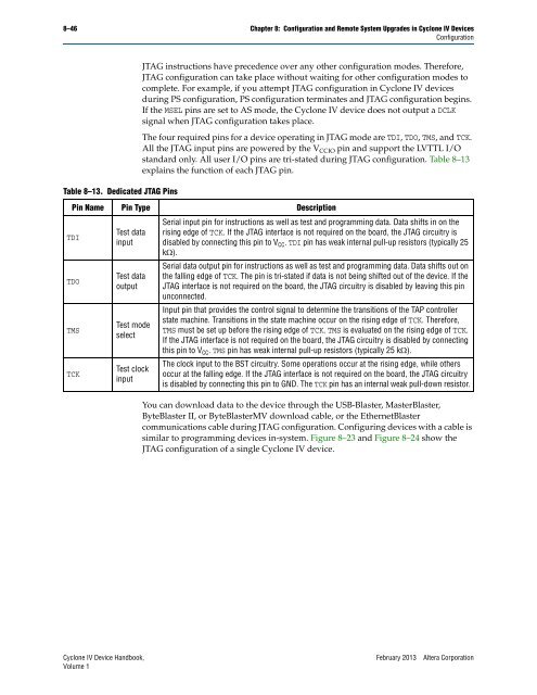
Table 8–13. Dedicated JTAG P<strong>in</strong>s<br />
JTAG <strong>in</strong>structions have precedence over any other configuration modes. Therefore,<br />
JTAG configuration can take place without wait<strong>in</strong>g for other configuration modes to<br />
complete. For example, if you attempt JTAG configuration <strong>in</strong> <strong>Cyclone</strong> <strong>IV</strong> devices<br />
dur<strong>in</strong>g PS configuration, PS configuration term<strong>in</strong>ates <strong>and</strong> JTAG configuration beg<strong>in</strong>s.<br />
If the MSEL p<strong>in</strong>s are set to AS mode, the <strong>Cyclone</strong> <strong>IV</strong> device does not output a DCLK<br />
signal when JTAG configuration takes place.<br />
The four required p<strong>in</strong>s for a device operat<strong>in</strong>g <strong>in</strong> JTAG mode are TDI, TDO, TMS, <strong>and</strong> TCK.<br />
All the JTAG <strong>in</strong>put p<strong>in</strong>s are powered by the V CCIO p<strong>in</strong> <strong>and</strong> support the LVTTL I/O<br />
st<strong>and</strong>ard only. All user I/O p<strong>in</strong>s are tri-stated dur<strong>in</strong>g JTAG configuration. Table 8–13<br />
expla<strong>in</strong>s the function of each JTAG p<strong>in</strong>.<br />
P<strong>in</strong> Name P<strong>in</strong> Type Description<br />
TDI<br />
TDO<br />
TMS<br />
TCK<br />
Test data<br />
<strong>in</strong>put<br />
Test data<br />
output<br />
Test mode<br />
select<br />
Test clock<br />
<strong>in</strong>put<br />
Serial <strong>in</strong>put p<strong>in</strong> for <strong>in</strong>structions as well as test <strong>and</strong> programm<strong>in</strong>g data. Data shifts <strong>in</strong> on the<br />
ris<strong>in</strong>g edge of TCK. If the JTAG <strong>in</strong>terface is not required on the board, the JTAG circuitry is<br />
disabled by connect<strong>in</strong>g this p<strong>in</strong> to V CC. TDI p<strong>in</strong> has weak <strong>in</strong>ternal pull-up resistors (typically 25<br />
k).<br />
Serial data output p<strong>in</strong> for <strong>in</strong>structions as well as test <strong>and</strong> programm<strong>in</strong>g data. Data shifts out on<br />
the fall<strong>in</strong>g edge of TCK. The p<strong>in</strong> is tri-stated if data is not be<strong>in</strong>g shifted out of the device. If the<br />
JTAG <strong>in</strong>terface is not required on the board, the JTAG circuitry is disabled by leav<strong>in</strong>g this p<strong>in</strong><br />
unconnected.<br />
Input p<strong>in</strong> that provides the control signal to determ<strong>in</strong>e the transitions of the TAP controller<br />
state mach<strong>in</strong>e. Transitions <strong>in</strong> the state mach<strong>in</strong>e occur on the ris<strong>in</strong>g edge of TCK. Therefore,<br />
TMS must be set up before the ris<strong>in</strong>g edge of TCK. TMS is evaluated on the ris<strong>in</strong>g edge of TCK.<br />
If the JTAG <strong>in</strong>terface is not required on the board, the JTAG circuitry is disabled by connect<strong>in</strong>g<br />
this p<strong>in</strong> to V CC. TMS p<strong>in</strong> has weak <strong>in</strong>ternal pull-up resistors (typically 25 k).<br />
The clock <strong>in</strong>put to the BST circuitry. Some operations occur at the ris<strong>in</strong>g edge, while others<br />
occur at the fall<strong>in</strong>g edge. If the JTAG <strong>in</strong>terface is not required on the board, the JTAG circuitry<br />
is disabled by connect<strong>in</strong>g this p<strong>in</strong> to GND. The TCK p<strong>in</strong> has an <strong>in</strong>ternal weak pull-down resistor.<br />
You can download data to the device through the USB-Blaster, MasterBlaster,<br />
ByteBlaster II, or ByteBlasterMV download cable, or the EthernetBlaster<br />
communications cable dur<strong>in</strong>g JTAG configuration. Configur<strong>in</strong>g devices with a cable is<br />
similar to programm<strong>in</strong>g devices <strong>in</strong>-system. Figure 8–23 <strong>and</strong> Figure 8–24 show the<br />
JTAG configuration of a s<strong>in</strong>gle <strong>Cyclone</strong> <strong>IV</strong> device.<br />
<strong>Cyclone</strong> <strong>IV</strong> Device H<strong>and</strong>book, February 2013 <strong>Altera</strong> Corporation<br />
Volume 1


