

Configuration and Remote System Upgrades in Cyclone IV ... - Altera
Configuration and Remote System Upgrades in Cyclone IV ... - Altera
Configuration and Remote System Upgrades in Cyclone IV ... - Altera

Create successful ePaper yourself
Turn your PDF publications into a flip-book with our unique Google optimized e-Paper software.
8–42 Chapter 8: <strong>Configuration</strong> <strong>and</strong> <strong>Remote</strong> <strong>System</strong> <strong>Upgrades</strong> <strong>in</strong> <strong>Cyclone</strong> <strong>IV</strong> Devices<br />
<strong>Configuration</strong><br />
To ensure that DCLK <strong>and</strong> DATA[0] are not left float<strong>in</strong>g at the end of the configuration,<br />
the MAX II device must drive them either high or low, whichever is convenient on<br />
your board. The DATA[0] p<strong>in</strong> is available as a user I/O p<strong>in</strong> after configuration. When<br />
you choose the FPP scheme <strong>in</strong> the Quartus II software, the DATA[0] p<strong>in</strong> is tri-stated by<br />
default <strong>in</strong> user mode <strong>and</strong> must be driven by the external host device. To change this<br />
default option <strong>in</strong> the Quartus II software, select the Dual-Purpose P<strong>in</strong>s tab of the<br />
Device <strong>and</strong> P<strong>in</strong> Options dialog box.<br />
The DCLK speed must be below the specified system frequency to ensure correct<br />
configuration. No maximum DCLK period exists, which means you can pause<br />
configuration by halt<strong>in</strong>g DCLK for an <strong>in</strong>def<strong>in</strong>ite amount of time.<br />
The external host device can also monitor the CONF_DONE <strong>and</strong> INIT_DONE p<strong>in</strong>s to ensure<br />
successful configuration. The CONF_DONE p<strong>in</strong> must be monitored by the external device<br />
to detect errors <strong>and</strong> to determ<strong>in</strong>e when programm<strong>in</strong>g is complete. If all configuration<br />
data is sent, but CONF_DONE or INIT_DONE has not gone high, the external device must<br />
reconfigure the target device.<br />
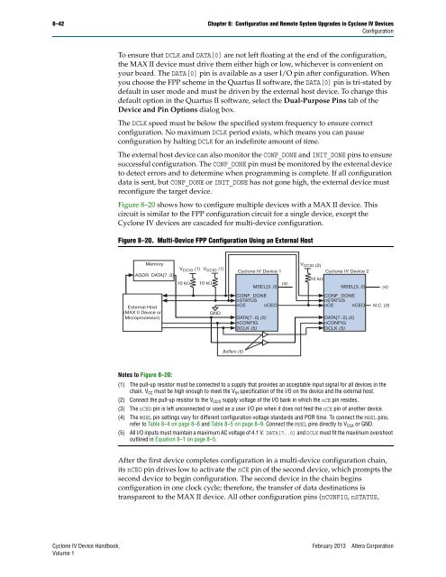
Figure 8–20 shows how to configure multiple devices with a MAX II device. This<br />
circuit is similar to the FPP configuration circuit for a s<strong>in</strong>gle device, except the<br />
<strong>Cyclone</strong> <strong>IV</strong> devices are cascaded for multi-device configuration.<br />
Figure 8–20. Multi-Device FPP <strong>Configuration</strong> Us<strong>in</strong>g an External Host<br />
Memory<br />
ADDR DATA[7..0]<br />
External Host<br />
(MAX II Device or<br />
Microprocessor)<br />
Notes to Figure 8–20:<br />
V CCIO (1) V CCIO (1)<br />
10 k<br />
10 k<br />
GND<br />
Buffers (5)<br />
<strong>Cyclone</strong> <strong>IV</strong> Device 1<br />
MSEL[3..0]<br />
CONF_DONE<br />
nSTATUS<br />
nCE nCEO<br />
DATA[7..0] (5)<br />
nCONFIG<br />
DCLK (5)<br />
VCCIO (2)<br />
<strong>Cyclone</strong> <strong>IV</strong> Device 2<br />
10 k<br />
CONF_DONE<br />
nSTATUS<br />
nCE nCEO N.C. (3)<br />
DATA[7..0] (5)<br />
nCONFIG<br />
DCLK (5)<br />
(1) The pull-up resistor must be connected to a supply that provides an acceptable <strong>in</strong>put signal for all devices <strong>in</strong> the<br />
cha<strong>in</strong>. VCC must be high enough to meet the VIH specification of the I/O on the device <strong>and</strong> the external host.<br />
(2) Connect the pull-up resistor to the VCCIO supply voltage of the I/O bank <strong>in</strong> which the nCE p<strong>in</strong> resides.<br />
(3) The nCEO p<strong>in</strong> is left unconnected or used as a user I/O p<strong>in</strong> when it does not feed the nCE p<strong>in</strong> of another device.<br />
(4) The MSEL p<strong>in</strong> sett<strong>in</strong>gs vary for different configuration voltage st<strong>and</strong>ards <strong>and</strong> POR time. To connect the MSEL p<strong>in</strong>s,<br />
refer to Table 8–4 on page 8–8 <strong>and</strong> Table 8–5 on page 8–9. Connect the MSEL p<strong>in</strong>s directly to VCCA or GND.<br />
(5) All I/O <strong>in</strong>puts must ma<strong>in</strong>ta<strong>in</strong> a maximum AC voltage of 4.1 V. DATA[7..0] <strong>and</strong> DCLK must fit the maximum overshoot<br />
outl<strong>in</strong>ed <strong>in</strong> Equation 8–1 on page 8–5.<br />
After the first device completes configuration <strong>in</strong> a multi-device configuration cha<strong>in</strong>,<br />
its nCEO p<strong>in</strong> drives low to activate the nCE p<strong>in</strong> of the second device, which prompts the<br />
second device to beg<strong>in</strong> configuration. The second device <strong>in</strong> the cha<strong>in</strong> beg<strong>in</strong>s<br />
configuration <strong>in</strong> one clock cycle; therefore, the transfer of data dest<strong>in</strong>ations is<br />
transparent to the MAX II device. All other configuration p<strong>in</strong>s (nCONFIG, nSTATUS,<br />
<strong>Cyclone</strong> <strong>IV</strong> Device H<strong>and</strong>book, February 2013 <strong>Altera</strong> Corporation<br />
Volume 1<br />
(4)<br />
MSEL[3..0]<br />
(4)


