

Configuration and Remote System Upgrades in Cyclone IV ... - Altera
Configuration and Remote System Upgrades in Cyclone IV ... - Altera
Configuration and Remote System Upgrades in Cyclone IV ... - Altera

Create successful ePaper yourself
Turn your PDF publications into a flip-book with our unique Google optimized e-Paper software.
8–48 Chapter 8: <strong>Configuration</strong> <strong>and</strong> <strong>Remote</strong> <strong>System</strong> <strong>Upgrades</strong> <strong>in</strong> <strong>Cyclone</strong> <strong>IV</strong> Devices<br />
<strong>Configuration</strong><br />
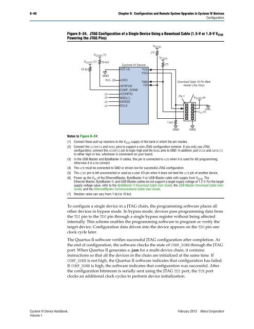
Figure 8–24. JTAG <strong>Configuration</strong> of a S<strong>in</strong>gle Device Us<strong>in</strong>g a Download Cable (1.5-V or 1.8-V V CCIO<br />
Power<strong>in</strong>g the JTAG P<strong>in</strong>s)<br />
V CCIO (1)<br />
10 kΩ<br />
Notes to Figure 8–24:<br />
V CCIO (1)<br />
10 kΩ<br />
GND<br />
N.C. (5)<br />
(2)<br />
(2)<br />
(2)<br />
(2)<br />
<strong>Cyclone</strong> <strong>IV</strong> Device<br />
nCE (4) TCK<br />
TDO<br />
nCEO<br />
nSTATUS<br />
CONF_DONE<br />
nCONFIG<br />
MSEL[ ]<br />
DATA[0]<br />
DCLK<br />
(1) Connect these pull-up resistors to the VCCIO supply of the bank <strong>in</strong> which the p<strong>in</strong> resides.<br />
(2) Connect the nCONFIG <strong>and</strong> MSEL p<strong>in</strong>s to support a non-JTAG configuration scheme. If you only use JTAG<br />
configuration, connect the nCONFIG p<strong>in</strong> to logic-high <strong>and</strong> the MSEL p<strong>in</strong>s to GND. In addition, pull DCLK <strong>and</strong> DATA[0]<br />
to either high or low, whichever is convenient on your board.<br />
(3) In the USB-Blaster <strong>and</strong> ByteBlaster II cables, this p<strong>in</strong> is connected to nCE when it is used for AS programm<strong>in</strong>g;<br />
otherwise it is a no connect.<br />
(4) The nCE must be connected to GND or driven low for successful JTAG configuration.<br />
(5) The nCEO p<strong>in</strong> is left unconnected or used as a user I/O p<strong>in</strong> when it does not feed the nCE p<strong>in</strong> of another device.<br />
(6) Power up the VCC of the EthernetBlaster, ByteBlaster II or USB-Blaster cable with supply from VCCIO. The<br />
Ethernet-Blaster, ByteBlaster II, <strong>and</strong> USB-Blaster cables do not support a target supply voltage of 1.2 V. For the target<br />
supply voltage value, refer to the ByteBlaster II Download Cable User Guide, the USB-Blaster Download Cable User<br />
Guide, <strong>and</strong> the EthernetBlaster Communications Cable User Guide.<br />
(7) Resistor value can vary from 1 k to 10 k.<br />
To configure a s<strong>in</strong>gle device <strong>in</strong> a JTAG cha<strong>in</strong>, the programm<strong>in</strong>g software places all<br />
other devices <strong>in</strong> bypass mode. In bypass mode, devices pass programm<strong>in</strong>g data from<br />
the TDI p<strong>in</strong> to the TDO p<strong>in</strong> through a s<strong>in</strong>gle bypass register without be<strong>in</strong>g affected<br />
<strong>in</strong>ternally. This scheme enables the programm<strong>in</strong>g software to program or verify the<br />
target device. <strong>Configuration</strong> data driven <strong>in</strong>to the device appears on the TDO p<strong>in</strong> one<br />
clock cycle later.<br />
The Quartus II software verifies successful JTAG configuration after completion. At<br />
the end of configuration, the software checks the state of CONF_DONE through the JTAG<br />
port. When Quartus II generates a .jam for a multi-device cha<strong>in</strong>, it conta<strong>in</strong>s<br />
<strong>in</strong>structions so that all the devices <strong>in</strong> the cha<strong>in</strong> are <strong>in</strong>itialized at the same time. If<br />
CONF_DONE is not high, the Quartus II software <strong>in</strong>dicates that configuration has failed.<br />
If CONF_DONE is high, the software <strong>in</strong>dicates that configuration was successful. After<br />
the configuration bitstream is serially sent us<strong>in</strong>g the JTAG TDI port, the TCK port<br />
clocks an additional clock cycles to perform device <strong>in</strong>itialization.<br />
<strong>Cyclone</strong> <strong>IV</strong> Device H<strong>and</strong>book, February 2013 <strong>Altera</strong> Corporation<br />
Volume 1<br />
TMS<br />
TDI<br />
(7)<br />
V CCIO<br />
V CCIO<br />
(7)<br />
1 kΩ<br />
GND<br />
Download Cable 10-P<strong>in</strong> Male<br />
Header (Top View)<br />
P<strong>in</strong> 1<br />
GND<br />
V CCIO (6)<br />
GND<br />
V IO (3)


